High Resolution Serial Output Circuit H Additional Manual Page 10
Additional Manual
High Resolution Serial Output
Circuit H
9/12
FANUC LTD
A-56731E-0089
Description Desig. Date Edit.
01 02.06.03 Kikuchi Taniguchi
title
Sheet
Draw. No.
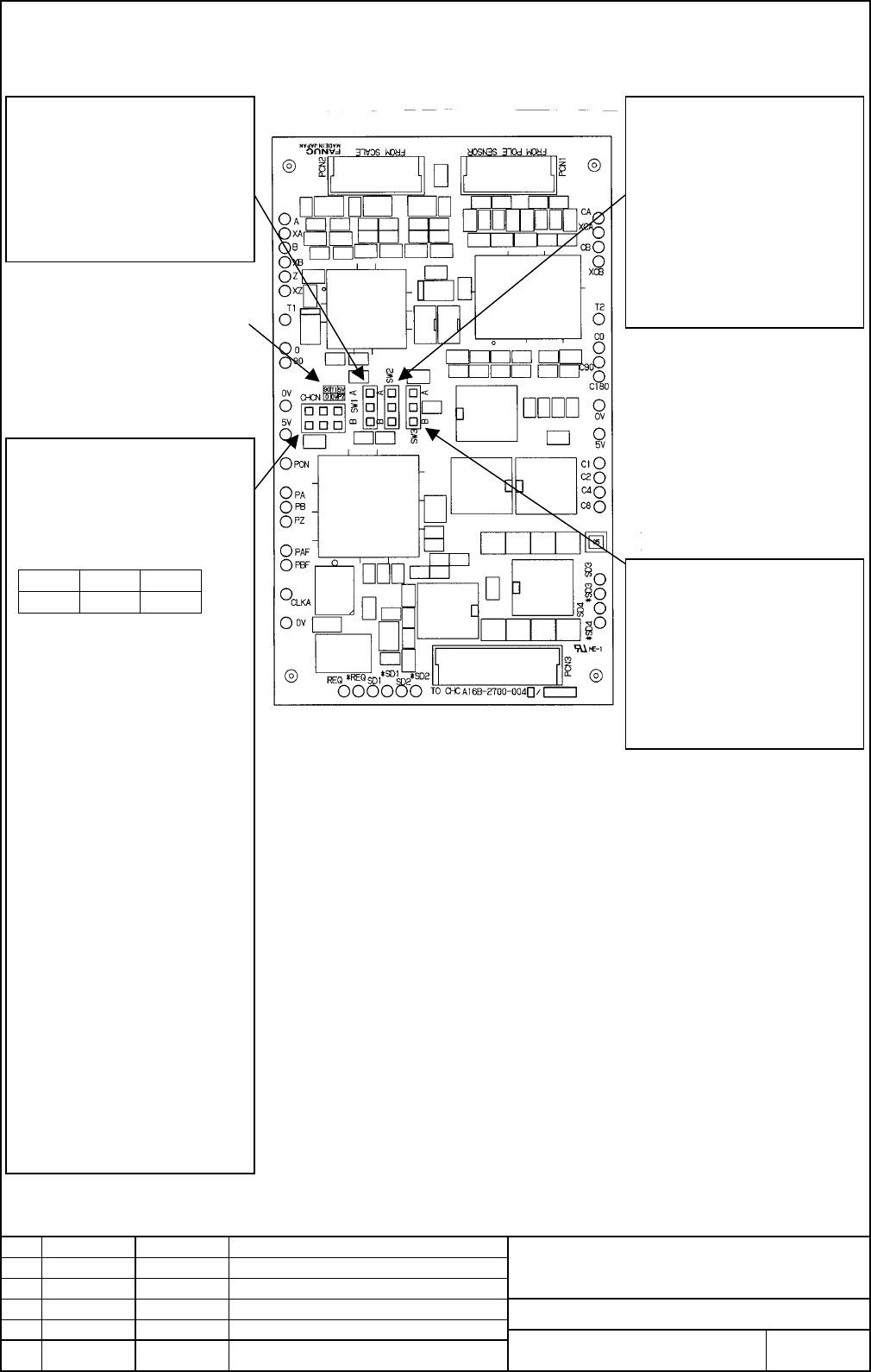
8. SETTING PINS AND CHECK PINS
Check pins in “CHCN”
Signals of 90, 0, T1, 0V, 5V,
and PZ can be observed in
these check pins.
The location is shown below.
90 T1 5V
0 0V PZ
90
Differentially amlified signal
from B and XB input signals.
90 = 2 x ( XB – B )
0
Differentially amplified signal
from A and XA input signals.
0 = 2 x ( XA – A )
T1
2.5V DC (=1/2 Vcc)
0V
Signal ground
5V
Power source
PZ
Comparated digital signal
from Z and XZ input signals
.
Check pins “CHCN” is added
on PCB version 06D or later.
Setting pin “SW1”
“A” setting:
CMAL function, by checking
position data and reference
signal, is valid.
“B” setting
A
bove function is invalid.
Setting pin “SW3”
“A” setting:
512 times interpolation
“B” setting
2048 times interpolation
Setting pin “SW3” is added
on PCB version 07E or later.
This means the location o
f
check pins (CHCN)
Setting pin “SW2”
“A” setting:
For analog reference signal
input.
“B” setting
For digital reference signal
input.
Setting pin “SW2” is added
on PCB version 06D or later.
Contents Summary of High Resolution Serial Output Circuit H Additional Manual
- Page 1TECHNICAL REPORT (MANUAL TMS03/016E Date May 2, 2003 General Manager of Servo Laboratory High Resolution Serial Output Circuit H 1. Distribute this report to the destinations marked with ○: ○ Your information ○ GE Fanuc-N, GE Fanuc-E Fanuc Robotics-NA, Fanuc Robotics-E CINCINNATI MILACRON ○ Machine
- Page 2High Resolution Serial Output Circuit H 1. Type of applied technical documents Name High Resolution Serial Output Circuit H Spec. No. / Version A-56731E-0089 2. Summary of Change New, Add, Group Name / Outline Applicable Correct, Delete Data Basic For Input Frequency 750kHz Add Function Optional Fun
- Page 33. GENERAL In this manual, the specifications and the connection diagram of High Resolution Serial Output Circuit H are described. 4. BLOCK DIAGRAM Separate type detector interface unit CNC High Resolution Serial Output Circuit H K2 K1 FSSB Encoder 5. SPECIFICATION AND FUNCTION (1 )Specification Ord
- Page 4(5) Resolution setting pin “SW3” It is able to set resolution by SW3 “A” setting : 512 times interpolation “B” setting : 2048 times interpolation “B” is set for “SW3” by using shorting pin at shipping. (6) Input specifications and examples of available linear encoders (6)-1 Input specifications A/B(
- Page 5(6)-2 Available Linear Encoders(Analog signal output type) Encoder Maker Encoder pitch of Maximum Scale Length Name signal [um] Velocity[m/min.] [mm] HEIDENHAIN LS486 20 120 70~ 2040 HEIDENHAIN LS186 20 120 240~ 3040 HEIDENHAIN LB382 100 120 440~30040 HEIDENHAIN LF183 4 48 140~ 3040 HEIDENHAIN LF481
- Page 66. CONNECTION DIAGRAM (1)Cable K1 Separate type High Resolution detector interface Serial Output unit Circuit H SD1 (3) (As for the connection XSD1 (4) of the CNC side,refer the REQ (1) manual of of each CNC) XREQ (2) 0V (9),(10),(11) 5V (12),(13),(14) SHIELD (15) 0V Connect to Earth Bar HIROSE RM21
- Page 7(2)Cable K2 High Resolution Encoder Serial output Circuit H A (5) XA (6) B (7) XB (8) Z (9) XZ (10) 0V (3),(4) 5V (1),(2) SHIELD (11) HIROSE RM15WTP-12P-(dia) Use wire that is specified by the encoder maker. Designate “dia” [mm] of the connector, according to diameter of the cable that is used. (5 ≦
- Page 8(3)Cable Length Design Design the length of cables as the sums of voltage drop by K1 and K2 becomes 0.2V or less. Note that voltage drop of K1 is caused by the total current consumption of High Resolution Serial Output Circuit and the encoder. [Example of calculation] Case that HEIDENHAIN LS486 is u
- Page 97. EXTERNAL DIMENSIONS title High Resolution Serial Output Circuit H Draw. No. A-56731E-0089 01 02.06.03 Kikuchi Taniguchi Sheet Edit. Date Desig. Description FANUC LTD 8/12
- Page 108. SETTING PINS AND CHECK PINS Setting pin “SW1” Setting pin “SW2” “A” setting: “A” setting: CMAL function, by checking For analog reference signal position data and reference input. signal, is valid. “B” setting “B” setting For digital reference signal Above function is invalid. input. Setting pin
- Page 119. PARAMETER SETTING Series and editions of applicable servo software : 90B0 / 17 and subsequent editions #7 #6 #5 #4 #3 #2 #1 #0 2274(FS16i) HP2048 2687 (FS15i) HP2048(#0) High Resolution Serial Output Circuit H is 0:Unavailable (512 times) 1:Available (2,048 times)(SW3 = “B” setting) (Note) This p
- Page 1210. FOR INPUT FREQUENCY 750kHz (1) Setting Pin SW3 “A” setting ( 512 times interpolation ) Cannot use “B” setting ( 2048 times interpolation ) for Input Frequency 750kHz. (2) Parameter Setting Series and editions of applicable servo software : 90B0 / 17 and subsequent editions #7 #6 #5 #4 #3 #2 #1 #
- Page 13【Number of position pulses / Position pulse conversion coefficient】Setting The amount of movement per motor revolution [mm] Detection unit of the sensor [mm] If the result of the above calculation does not fall in the setting range(0 to 32767)for the number of position pulses, use “position feedback