Servo Amplifier Alpha i Series Descriptions Page 260
Descriptions
9.CONNECTION B-65282EN/05
- 238 -
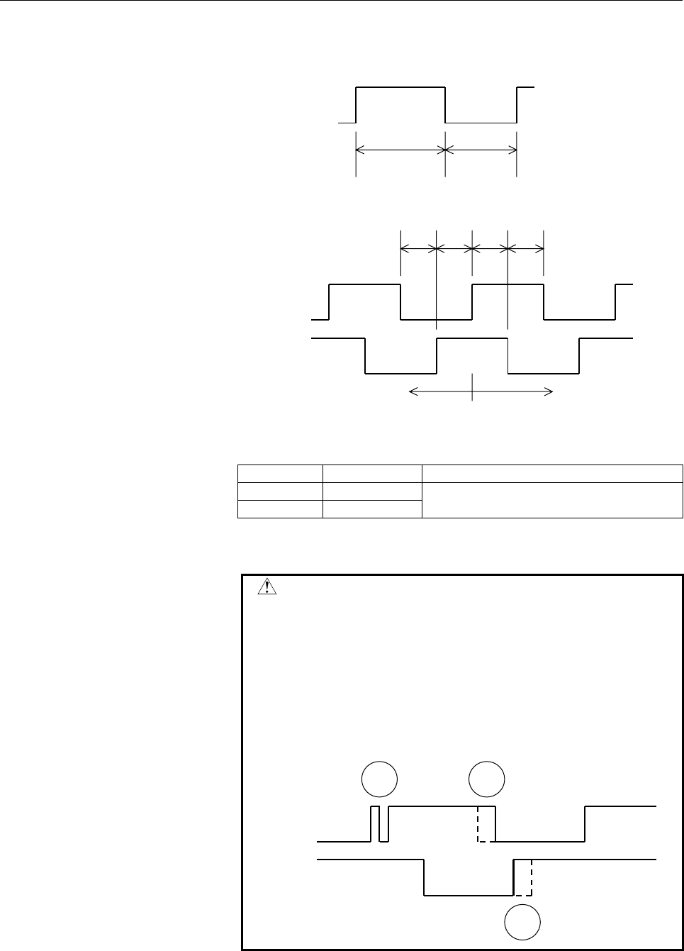
Phase A/B signal
Width of phase A/B signal
PA,*PA,PB,*PB
Tpwh Tpwl
Phase difference between phase A and phase B
PA
Tpw0
CCW directionCW direction
Tpw1 Tpw2 Tpw3
PB
*PA and *PB represent the negative logic signals of PA and PB,
respectively.
Symbol Specification Remark
Tpwh, Tpwl Min 636ns
Tpw0,1,2,3 Min 636ns
Including a maximum of driver rising/falling
delay time skew (30 ns)
This specification does not include the effect of the cable capacity
and the skew due to delay on the receiver side.
CAUTION
As shown in state A below, a waveform may be
distorted at the edge of phase A or B.
In addition, the edge may be encountered too late
or too early as shown in state B or C. Even in these
states, the minimum time is defined according to
the specifications described on the previous page,
such as the pulse width and the difference between
phase A and phase B.
PA
PB
A
C
B
Contents Summary of Servo Amplifier Alpha i Series Descriptions
- Page 1FANUC SERVO AMPLIF IER @* series DESCRIPTIONS B-65282EN/05
- Page 2Ȧ No part of this manual may be reproduced in any form. Ȧ All specifications and designs are subject to change without notice. In this manual we have tried as much as possible to describe all the various matters. However, we cannot describe all the matters which must not be done, or which cannot be
- Page 3B-65282EN/05 SAFETY PRECAUTIONS SAFETY PRECAUTIONS This "Safety Precautions" section describes the precautions which must be observed to ensure safety when using FANUC servo amplifiers (including spindle amplifiers). Users of any control motor amplifier model are requested to read the "Safety Precau
- Page 4SAFETY PRECAUTIONS B-65282EN/05 1.1 DEFINITION OF WARNING, CAUTION, AND NOTE This manual includes safety precautions for protecting the user and preventing damage to the machine. Precautions are classified into Warning and Caution according to their bearing on safety. Also, supplementary information
- Page 5B-65282EN/05 SAFETY PRECAUTIONS 1.2 WARNINGS AND CAUTIONS RELATING TO MOUNTING 1.2.1 Warning WARNING - Check the specification code of the amplifier. Check that the delivered amplifier is as originally ordered. - Mount a ground fault interrupter. To guard against fire and electric shock, fit the fac
- Page 6SAFETY PRECAUTIONS B-65282EN/05 WARNING - Close the amplifier cover after completing the wiring. Leaving the cover open presents a danger of electric shock. - Do not disassemble the amplifier. - Ensure that the cables used for the power supply lines and power lines are of the appropriate diameter an
- Page 7B-65282EN/05 SAFETY PRECAUTIONS 1.2.2 Caution CAUTION - Do not step or sit on the amplifier. Also, do not stack unpacked amplifiers on top of each other. - Use the amplifier in an appropriate environment. See the allowable ambient temperatures and other requirements, given in the corresponding descr
- Page 8SAFETY PRECAUTIONS B-65282EN/05 CAUTION - Check that the amplifier is securely mounted in the power magnetic cabinet. If any clearance is left between the power magnetic cabinet and the surface on which the amplifier is mounted, dust entering the gap may build up and prevent the normal operation of
- Page 9B-65282EN/05 SAFETY PRECAUTIONS 1.2.3 Note NOTE - Keep the nameplate clearly visible. - Keep the legend on the nameplate clearly visible. - After unpacking the amplifier, carefully check for any damage. - Mount the amplifier in a location where it can be easily accessed periodic inspection and daily
- Page 10SAFETY PRECAUTIONS B-65282EN/05 1.3 WARNINGS AND CAUTIONS RELATING TO A PILOT RUN 1.3.1 Warning WARNING - Before turning on the power, check that the cables connected to the power magnetic cabinet and amplifier, as well as the power lines and power supply lines, are securely connected. Also, check t
- Page 11B-65282EN/05 SAFETY PRECAUTIONS 1.3.2 Caution CAUTION - Note whether an alarm status relative to the amplifier is displayed at power-up or during operation. If an alarm is displayed, take appropriate action as explained in the maintenance manual. If the work to be done requires that the door of the
- Page 12SAFETY PRECAUTIONS B-65282EN/05 1.4 Warnings and Cautions Relating to Maintenance 1.4.1 Warning WARNING - Read the maintenance manual carefully and ensure that you are totally familiar with its contents. The maintenance manual describes daily maintenance and the procedures to be followed in the even
- Page 13B-65282EN/05 SAFETY PRECAUTIONS WARNING - Notes on replacing the battery of the absolute Pulsecoder Replace the battery only while the power is on. If the battery is replaced while the power is turned off, the stored absolute positioning data will be lost. Some αi series servo amplifier modules have
- Page 14SAFETY PRECAUTIONS B-65282EN/05 1.4.2 Caution CAUTION - Ensure that all required components are mounted. When replacing a component or PC board, check that all components, including the snubber capacitor, are correctly mounted. If the snubber capacitor is not mounted, for example, the IPM will be da
- Page 15B-65282EN/05 SAFETY PRECAUTIONS 1.4.3 Note NOTE - Ensure that the battery connector is correctly inserted. If the power is shut off while the battery connector is not connected correctly, the absolute position data for the machine will be lost. - Store the manuals in a safe place. The manuals should
- Page 16
- Page 17B-65282EN/05 TABLE OF CONTENTS TABLE OF CONTENTS SAFETY PRECAUTIONS .......................................................................... s-1 1 CONFIGURATION..................................................................................1 1.1 FEATURES OF THE SERVO AMPLIFIER αi SERIES.........
- Page 18TABLE OF CONTENTS B-65282EN/05 3.1.3.7 Regenerative discharge unit ...............................................................................61 3.1.3.8 Cables ................................................................................................................62 3.1.3.9 Circuit break
- Page 19B-65282EN/05 TABLE OF CONTENTS 5.3.1 Separation of Signal Lines..................................................................................... 95 5.3.2 Cable Clamp and Shield Processing...................................................................... 96 5.3.3 Others.......................
- Page 20TABLE OF CONTENTS B-65282EN/05 9.3.1.2 Details of short bar K2 .....................................................................................178 9.3.1.3 Details of cable K3...........................................................................................182 9.3.1.4 Details of cable K
- Page 21B-65282EN/05 TABLE OF CONTENTS 10.2 POWER LINE SWITCH UNIT....................................................................254 10.2.1 Overview.............................................................................................................. 254 10.2.2 Specification ...................
- Page 22TABLE OF CONTENTS B-65282EN/05 D.2 SERVO CABLE LENGTH (WHEN RECOMMENDED CABLES ARE USED) .....................................327 E POWER LINE FOR SERVO MOTOR AND AMPLIFIER ....................328 E.1 SELECTING A POWER CABLE................................................................329 E.2 SAMP
- Page 23B-65282EN/05 1.CONFIGURATION 1 CONFIGURATION -1-
- Page 241.CONFIGURATION B-65282EN/05 1.1 FEATURES OF THE SERVO AMPLIFIER αi SERIES The servo amplifier αi series employs a modular structure, and is thinner, conserves more space, outputs less heat, and saves more energy than the conventional servo amplifier α series. Compact (1) By employing a leading-edge
- Page 25B-65282EN/05 1.CONFIGURATION 1.2 CONFIGURATION The FANUC αi series consists of the following units and parts: 1.2.1 200-V Input Series (1) Power supply module (PSM) ........................................... (Basic) (2) Power supply module (PSMR) ....................................... (Basic) [reg
- Page 261.CONFIGURATION B-65282EN/05 Basic configuration using PSM (example) Power supply Spindle amplifier Servo amplifier module module module PSM SPM SVM2 DC link (300VDC) Circuit 200R,200S breaker 2 1φ Circuit Magnetic AC reactor breaker 2 contactor 3φ 200 to 240 VAC 3φ fan motor 3φ Lightning Lightning
- Page 27B-65282EN/05 1.CONFIGURATION Basic configuration using PSMR (example) Power supply Spindle amplifier Servo amplifier module module module PSMR SPM SVM2 DC link (300VDC) Circuit 200R,200S breaker 2 1φ Circuit Magnetic AC line Regenerative breaker 1 contactor filter discharge unit 3φ 200 to 240 VAC 3φ
- Page 281.CONFIGURATION B-65282EN/05 1.2.2 400-V Input Series (1) Power supply module (PSM-HV).................................... (Basic) (2) Servo amplifier module (SVM-HV) ................................ (Basic) (3) Spindle amplifier module (SPM-HV).............................. (Basic) (4) AC reactor..
- Page 29B-65282EN/05 1.CONFIGURATION Basic configuration using PSM-HV (example) Power supply Spindle amplifier Servo amplifier module module module PSM-HV SPM-HV SVM2-HV DC link (300VDC) Circuit 1φ 200R,200S breaker 2 200 to 240 VAC Lightning Lightning 3φ surge surge protector protector Circuit Magnetic AC
- Page 301.CONFIGURATION B-65282EN/05 1.3 MODULE NAME Power supply module (PSM) The power supply module (PSM) supplies main power for driving motors and supplies control power to other modules. A PSM specification is selected according to the servo motors and spindle motor used. There are three types of powe
- Page 31B-65282EN/05 1.CONFIGURATION Servo amplifier module (SVM) The servo amplifier module (SVM) is used to drive servo motors. An SVM is selected according to the servo motor(s) connected to the SVM. There are two types of servo amplifier module, as follows: <1> Servo amplifier module (SVM) This module d
- Page 321.CONFIGURATION B-65282EN/05 1.4 LINEUP 200-V input type Size PSM PSMR SPM SPMC SVM1 SVM2 SVM3 60mm-wide 3i 4/4i 4/4/4i 20i Without external fin 20/20i 20/20/20i 20/40i 40i 60mm-wide 2.2i 2.2i 40/40i 5.5i 80i 20/20/40i With external fin 5.5i 5.5i 5.5i 40/80i 160i 80/80i 90mm-wide 11i 11i 11i 80/160i
- Page 33B-65282EN/05 1.CONFIGURATION 60mm-wide 60mm-wide 90mm-wide 150mm-wide 300mm-wide Without external fin With external fin With external fin With external fin With external fin 380 60 60 90 150 300 172 100 - 11 -
- Page 342.SPECIFICATIONS B-65282EN/05 2 SPECIFICATIONS - 12 -
- Page 35B-65282EN/05 2.SPECIFICATIONS 2.1 INPUT POWER Power supply of 200-V input series (1) Power specification Item Specification Power supply voltage for Three-phase 200 VAC to 240 VAC the main circuit Power supply voltage for Single-phase 200 VAC to 240 VAC (input from the control circuit connector CX1A
- Page 362.SPECIFICATIONS B-65282EN/05 (3) It is recommended that a capacitor unit for power-factor improvement not be installed. This is because the capacitor unit for power-factor improvement may adversely affect power regeneration. (4) The rated output of the motor is guaranteed for the rated input voltag
- Page 37B-65282EN/05 2.SPECIFICATIONS Power supply of 400-V input series (1) Power specification Item Specification Three-phase 400 VAC to 480 VAC Star connection, neutral grounding (For details, see Items (5) and (6).) R Power supply voltage for N S the main circuit T G Single-phase 200 VAC to 240 VAC (inp
- Page 382.SPECIFICATIONS B-65282EN/05 (2) The control circuit power to the power supply module (power input to CX1A) must be turned on before the power to the CNC is turned on or within 500 ms after the power to the CNC is turned on. (3) It is recommended that a capacitor unit for power-factor improvement n
- Page 39B-65282EN/05 2.SPECIFICATIONS (6) Example of connecting the power supply of the main circuit No. Power system Power specification Power supply of amplifier 1 TN-power system • Star connection • Directly connectable to the power supply • Neutral grounding on the power (No transformer is required.) su
- Page 402.SPECIFICATIONS B-65282EN/05 (a) TN-power system No. Power system Power specification Power supply of amplifier 1 TN-power system • Star connection • Directly connectable to the power supply • Neutral grounding on the power (No transformer is required.) supply side • PE provided on the power line •
- Page 41B-65282EN/05 2.SPECIFICATIONS (b) TN-power system No. Power system Power specification Power supply of amplifier 2 TN-power system • Star connection • The power supply voltage is decreased • Neutral grounding on the power with an auto-transformer. supply side • PE provided on the power line • Power
- Page 422.SPECIFICATIONS B-65282EN/05 (c) TN-power system No. Power system Power specification Power supply of amplifier 3 TN-power system • Delta connection • An isolating-transformer is used. • Single-phase grounding on the • A star connection is made on the power supply side secondary side of an isolatin
- Page 43B-65282EN/05 2.SPECIFICATIONS (d) TT-power system No. Power system Power specification Power supply of amplifier 4 TT-power system • Star connection • An isolating-transformer is used. • Neutral grounding on the power • A star connection is made on the supply side secondary side of an isolating-tran
- Page 442.SPECIFICATIONS B-65282EN/05 (e) TT-power system No. Power system Power specification Power supply of amplifier 5 TT-power system • Delta connection • An isolating-transformer is used. • Single-phase grounding on the • A star connection is made on the secondary power supply side side of an isolatin
- Page 45B-65282EN/05 2.SPECIFICATIONS (f) IT-power system No. Power system Power specification Power supply of amplifier 6 IT-power system • Star connection • An isolating-transformer is used. • No direct ground connection • A star connection is made on the secondary made on the power supply side side of an
- Page 462.SPECIFICATIONS B-65282EN/05 (g) IT-power system No. Power system Power specification Power supply of amplifier 7 IT-power system • Delta connection • An isolating-transformer is used. • No direct ground connection • A star connection is made on the secondary made on the power supply side side of a
- Page 47B-65282EN/05 2.SPECIFICATIONS (7) Control power supply connection • Specification of the control power supply voltage for the αHVi series servo amplifier Single-phase 200 VAC to 240 VAC (-15%, +10%) • When the power supply has a neutral point, power can be supplied from the neutral point and phase v
- Page 482.SPECIFICATIONS B-65282EN/05 2.2 ENVIRONMENTAL CONDITIONS The servo amplifier αi series must be installed in a sealed type cabinet to satisfy the following environmental requirements: (1) Ambient Temperature Ambient temperature of the unit : 0 to 55°C (at operation) -20 to 60°C (at keeping and tran
- Page 49B-65282EN/05 2.SPECIFICATIONS (d) Current lines and signal lines must be separated and noise must be suppressed. See the section 5.3 and the connection manual for each CNC for details. (f) Each amplifier must be installed vertically. (g) Servo amplifiers are to be arranged horizontally. When arrangi
- Page 502.SPECIFICATIONS B-65282EN/05 SVM2-20/40i to 160/160i 100% 80% rated output current Percentage of 60% 40% 20% 0% 0 10 20 30 40 50 60°°C Ambient temperature SVM1-4i to 20i SVM2-4/4i to SVM2-20/20i SVM3-4/4/4i to SVM3-20/20/40i 100% 80% rated output current Percentage of 60% 40% 20% 0% 0 10 20 30 40 5
- Page 51B-65282EN/05 2.SPECIFICATIONS SVM1-10HVi to 80HVi 100% 80% rated output current Percentage of 60% 40% 20% 0% 0 10 20 30 40 50 60°°C Ambient temperature SVM1-180HVi to SVM1-360HVi 100% 80% rated output current Percentage of 60% 40% 20% 0% 0 10 20 30 40 50 60°°C Ambient temperature SVM2-10/10HVi to 20
- Page 522.SPECIFICATIONS B-65282EN/05 SVM2-20/40HVi to 80/80HVi 100% 80% rated output current Percentage of 60% 40% 20% 0% 0 10 20 30 40 50 60°°C Ambient temperature (b) SPindle amplifier module SPM-2.2i to 55i SPM-5.5HVi to 100HVi 30 min. Available operating time 20 min. at short-term rating 10 min. 0 0 10
- Page 53B-65282EN/05 2.SPECIFICATIONS 2.3 SPECIFICATIONS OF THE MODULES 2.3.1 Power Supply Module (PSM) 200-V input series - power supply regeneration (PSM) Model PSM-5.5i PSM-11i PSM-15i PSM-26i PSM-30i PSM-37i PSM-55i Item Power supply Main circuit 200 to 240VAC +10%,-15%,3φ 50/60Hz, ±1Hz (Note) Control p
- Page 542.SPECIFICATIONS B-65282EN/05 400-V input series - power supply regeneration (SVM) Model PSM-11HVi PSM-18HVi PSM-30HVi PSM-45HVi PSM-75HVi PSM-100HVi Item Power supply Main circuit 400 to 480VAC +10%,-15%,3φ 50/60Hz, ±1Hz (Note) Control power 200 to 240VAC +10%,-15%,1φ 50/60Hz, ±1Hz Power equipment
- Page 55B-65282EN/05 2.SPECIFICATIONS 2.3.2 Servo Amplifier Module (SVM) Specifications (common) Item Specifications Main circuit control Sine-wave PWM control with transistor (IGBT) bridge method Applicable CNC CNC of the i series (MODEL B) with the FSSB interface 200-V input series - SVM 1-axis Rated outp
- Page 562.SPECIFICATIONS B-65282EN/05 200-V input series - SVM 3-axis Rated output current Nominal current limit Name Axis [Arms] [Apeak] L 1.5 4 SVM3-4/4/4i M 1.5 4 N 1.5 4 L 6.5 20 SVM3-20/20/20i M 6.5 20 N 6.5 20 L 6.5 20 SVM3-20/20/40i M 6.5 20 N 13 40 400-V input series - SVM 1-axis Rated output curren
- Page 57B-65282EN/05 2.SPECIFICATIONS 2.3.3 Spindle Amplifier Module (SPM) 200-V input series Model SPM- SPM- SPM- SPM- SPM- SPM- SPM- SPM- SPM- Item 2.2i 5.5i 11i 15i 22i 26i 30i 45i 55i Rated output (*1) 13A 27A 48A 63A 95A 111A 133A 198A 250A Main circuit control Sine-wave PWM control with transistor (IG
- Page 582.SPECIFICATIONS B-65282EN/05 Types (A and B) of SPMs and sensors applicable to each type Either of two SPM models, types A and B, is available for each detector on the spindle to be used. The following lists combinations of an SPM type, applicable sensors, and functions. Configuration Remarks 1 2 3
- Page 59B-65282EN/05 2.SPECIFICATIONS SPM and CNC matching SPM and CNC matching conforms to the CNC i series model B. Other functions SPM TYPE SPM TYPE Remarks A B Analog output of load meter O O Connector JY1 and speedometer Analog override input O O Connector JY1 Position coder signal output O Connector J
- Page 602.SPECIFICATIONS B-65282EN/05 2.3.4 αCi Spindle Amplifier Module (SPMC) 200-V input series Model SPMC-2.2i SPMC-5.5i SPMC-11i SPMC-15i SPMC-22i Item Rated output 13A 27A 48A 63A 95A Main circuit control method Sine-wave PWM control with transistor (IGBT) bridge Speed control range Speed ratio 1:50 S
- Page 61B-65282EN/05 2.SPECIFICATIONS SPM and CNC matching SPM and CNC matching conforms to the CNC i series model B. Other functions SPMC Remarks One-channel analog output of either load meter or speedometer O Connector JY1 (Selected by parameter setting) Analog override input O Connector JY1 - 39 -
- Page 622.SPECIFICATIONS B-65282EN/05 2.4 WEIGHT PSM Model Weight PSMR-3i 2.6kg PSMR-5.5i 4.3kg PSM-5.5i 4.9kg PSM-11i, 15i, 11HVi, 18HVi 6.3kg PSM-26i, 30i, 37i, 30HVi, 45HVi 10.7kg PSM-55i, 75HVi, 100HVi 22.0kg AC reactor Model Weight A81L-0001-0083#3C (For PSMR-3i) 1.1kg A81L-0001-0101#C (For PSMR-5.5i)
- Page 63B-65282EN/05 2.SPECIFICATIONS SPM Model Weight SPM-2.2i, SPMC-2.2i 4.9Kg SPM-5.5i , 5.5HVi, SPMC-5.5i 6.1Kg SPM-11i, 15i, 11HVi, 15HVi 6.3Kg SPMC-11i, 15i, SPM-22i, 26i, 30i, 30HVi, 45HVi 10.7Kg SPMC-22i SPM-45i, 55i, 75HVi, 100HVi 22.0Kg - 41 -
- Page 643.ORDERING INFORMATION B-65282EN/05 3 ORDERING INFORMATION - 42 -
- Page 65B-65282EN/05 3.ORDERING INFORMATION 3.1 SERVO AMPLIFIER 3.1.1 200-V Input Series 3.1.1.1 Power supply module (PSM) Category Ordering number Name Remarks A06B-6110-H006 PSM-5.5i A06B-6110-H011 PSM-11i A06B-6110-H015 PSM-15i Standard A06B-6110-H026 PSM-26i A06B-6110-H030 PSM-30i A06B-6110-H037 PSM-37i
- Page 663.ORDERING INFORMATION B-65282EN/05 3.1.1.3 Servo amplifier module (SVM) SVM 1-axis Category Ordering number Name Remarks A06B-6114-H103 SVM1-20i A06B-6114-H104 SVM1-40i Standard A06B-6114-H105 SVM1-80i A06B-6114-H106 SVM1-160i A06B-6114-H109 SVM1-360i SVM 2-axis Category Ordering number Name Remark
- Page 67B-65282EN/05 3.ORDERING INFORMATION 3.1.1.4 Spindle amplifier module (SPM) Ordering numbers depend on the detectors being used (function). (1) TYPE A (1 spindle sensor input) Category Ordering number Name Remarks A06B-6111-H002#H550 SPM-2.2i A06B-6111-H006#H550 SPM-5.5i A06B-6111-H011#H550 SPM-11i A
- Page 683.ORDERING INFORMATION B-65282EN/05 3.1.2 400-V Input Series 3.1.2.1 Power supply module (PSM-HV) Category Ordering number Name Remarks A06B-6120-H011 PSM-11HVi A06B-6120-H018 PSM-18HVi A06B-6120-H030 PSM-30HVi Standard A06B-6120-H045 PSM-45HVi A06B-6120-H075 PSM-75HVi A06B-6120-H100 PSM-100HVi NOTE
- Page 69B-65282EN/05 3.ORDERING INFORMATION 3.1.2.2 Servo amplifier module (SVM-HV) SVM 1-axis Category Ordering number Name Remarks A06B-6124-H102 SVM1-10HVi A06B-6124-H103 SVM1-20HVi A06B-6124-H104 SVM1-40HVi Standard A06B-6124-H105 SVM1-80HVi A06B-6124-H106 SVM1-180HVi A06B-6124-H109 SVM1-360HVi SVM 2-ax
- Page 703.ORDERING INFORMATION B-65282EN/05 3.1.2.3 Spindle amplifier module (SPM-HV) Ordering numbers depend on the detectors being used (function). (1) TYPE A (1 spindle sensor input) Category Ordering number Name Remarks A06B-6121-H006#H550 SPM-5.5HVi A06B-6121-H011#H550 SPM-11HVi A06B-6121-H015#H550 SPM
- Page 71B-65282EN/05 3.ORDERING INFORMATION 3.1.3 Others 3.1.3.1 AC reactor Category Ordering number Name Remarks A81L-0001-0155 PSM-5.5i, 11i A81L-0001-0156 PSM-15i A81L-0001-0157 PSM-26i A81L-0001-0158 PSM-30i Standard A81L-0001-0159 PSM-37i A81L-0001-0160 PSM-55i A81L-0001-0163 PSM-11HVi, 18HVi A81L-0001
- Page 723.ORDERING INFORMATION B-65282EN/05 3.1.3.4 Connectors The ordering drawing number of the connectors required for connection of input/output signals of each module, and the configuration of each connector, are shown below. The "Use" column of the table indicates connection symbol K*, which is descri
- Page 73B-65282EN/05 3.ORDERING INFORMATION (3) For power supply module (PSM) Category Ordering number Quantity Use Connection tool Housing: 1 pcs./module Contact crimping tool Standard A06B-6071-K203 K3, K6, K7 Contact: 7 pcs. A06B-6110-K220#D3L (4) For servo amplifier module (SVM) Category Ordering number
- Page 743.ORDERING INFORMATION B-65282EN/05 Connection tools Connector connection tools are indicated below with their ordering numbers for purchase from FANUC. The connection tools can also be directly purchased from each manufacturer. (a) Connectors manufactured by Tyco Electronics AMP D-2100 series (for
- Page 75B-65282EN/05 3.ORDERING INFORMATION Connector configuration - Configuration of A06B-6110-K210 Connector name Manufacturer Part number Quantity Use Dimensions CXA2A 1-1318119-4 (housing) 1 C(d) AMP Japan, Ltd. For PSM interface CXA2B 131807-1 (contact) 8 - - Configuration of A06B-6110-K211 Connector
- Page 763.ORDERING INFORMATION B-65282EN/05 - Configuration of A06B-6110-K201#XYL Connector name Manufacturer Part number Quantity Use Dimensions 3-917807-2 (housing) 1 - CZ2M AMP Japan, Ltd. For motor power 1318697-6 (contact) 4 - - Configuration of A06B-6110-K202#YYSS Connector name Manufacturer Part numb
- Page 77B-65282EN/05 3.ORDERING INFORMATION - Configuration of A06B-6078-K222 (solder type, side cable type) Connector name Manufacturer Part number Quantity Use Dimensions JY1 FI40B-20S (connector) 1 C(f) JYA2 Hirose Electric See below. JYA3 Co., Ltd. FI-20-CVS5 (case) 1 C(i) JYA4 Use Mi sensor, MZi sensor
- Page 783.ORDERING INFORMATION B-65282EN/05 3.1.3.5 Fuses The ordering numbers of fuses used with each module (PSM, SVM, SPM) are indicated below. (1) For control power supply for PSM Category Ordering number Remarks Manufacturer : Daito Communication Apparatus Co., Ltd. Optional A06B-6077-K250 Manufacturer
- Page 79B-65282EN/05 3.ORDERING INFORMATION 3.1.3.6 Power transformer When a power supply module of the 200V input series is used in an area where the input voltage is not within the range of 200 to 230VAC, a power transformer is required. The ordering drawing numbers and specifications of power transformer
- Page 803.ORDERING INFORMATION B-65282EN/05 Specifications of power transformers manufactured by FANUC Power transformer for PSM Model PSM-37i PSM-5.5i PSM-11i PSM-15i PSM-26i, 30i PSM-55i Item (at 45kw output) Ordering drawing A06B-6052-J001 A06B-6044-J006 A06B-6044-J007 A06B-6044-J010 A06B-6044-J015 numbe
- Page 81B-65282EN/05 3.ORDERING INFORMATION Power transformer for PSMR Model PSMR-3i PSMR-3i PSMR-5.5i PSMR-5.5i Item (at 2kw output) (at 3kw output) (at 5.5kw output) (at 7.5kw output) Ordering drawing A80L-0024-0006 A80L-0026-0003 A06B-6052-J001 A06B-6044-J006 number FANUC drawing A80L-0024-0006 A80L-0026
- Page 823.ORDERING INFORMATION B-65282EN/05 Connecting a power transformer Power transformers must be set according to the supply voltage used. (a) Connection points of power transformers for PSM-5.5i, PSM-11i, PSM-15i, PSM-26i, PSM-30i, and PSM-37i Supply voltage Connection points at the primary Remarks 38
- Page 83B-65282EN/05 3.ORDERING INFORMATION 3.1.3.7 Regenerative discharge unit Whenever a PSMR (resistance regeneration type power supply module) is used, a regenerative discharge unit must be specified. For how to select the regenerative discharge unit, see Subsection 4.4.4. Category Name Ordering number
- Page 843.ORDERING INFORMATION B-65282EN/05 3.1.3.8 Cables DC link short bar Category Ordering number Applicable terminal-to-terminal distance A06B-6078-K801 90mm (86mm - 94mm) A06B-6078-K803 64mm (60mm - 68mm) Optional A06B-6078-K840 154mm (150mm - 158mm) A06B-6078-K841 300mm (298mm - 302mm) A06B-6078-K842
- Page 85B-65282EN/05 3.ORDERING INFORMATION 3.1.3.9 Circuit breaker and magnetic contactor The circuit breaker and magnetic contactor capacities are determined by the power supply module specifications. The ordering drawing numbers and specifications of the circuit breakers and magnetic contactors are shown
- Page 863.ORDERING INFORMATION B-65282EN/05 For PSM-HV Circuit Circuit Circuit Magnetic PSM name Remarks breaker 1 breaker 2 breaker 3 contactor PSM-11HVi 20A 20A PSM-18HVi 45A 30A PSM-30HVi 75A 55A 3A 3A PSM-45HVi 125A 70A PSM-75HVi 200A 120A PSM-100HVi 250A 140A NOTE 1 For the installation positions of th
- Page 87B-65282EN/05 3.ORDERING INFORMATION Ordering drawing numbers of circuit breakers Outline Circuit breaker Circuit breaker cover Category Model Ordering number drawing specification specification PSMR-3i Fuji Electric A06B-6077-K101 8.1.7(a) Fuji Electric BZ-TB20B-3 PSM-11HVi EA53B/30 PSMR-5.5i Fuji E
- Page 883.ORDERING INFORMATION B-65282EN/05 3.1.3.10 Lightning surge protector To protect equipment from surge voltages caused by lightning, install a lightning surge protector between lines and between a line and ground. For how to install protectors, see Appendix A. Lightning surge protector specification
- Page 89B-65282EN/05 3.ORDERING INFORMATION 3.1.3.11 Noise filter A noise filter must be installed in the PSM input section to satisfy the requirements of the EMC Directives which are now being enforced in the EU countries. Ordering Outline Category Model Specification number drawing Manufactured by Okaya P
- Page 903.ORDERING INFORMATION B-65282EN/05 3.1.3.12 Sensors for spindle α Positioncoder Ordering Category Name Remarks number α Positioncoder A860-0309-T302 68, 10,000min-1 Optional Connector kit A06B-6088-K211 Straight type α Positioncoder S (analog output type) Ordering Category Name Remarks number α Pos
- Page 91B-65282EN/05 3.ORDERING INFORMATION 3.1.3.14 Battery for absolute Pulsecoder For connection of a battery for an absolute Pulsecoder, two methods are available. For each method, options are available. NOTE 1 A battery needs to be maintained periodically. So, [connection type 1] is recommended because
- Page 924.HOW TO SELECT THE MODULE B-65282EN/05 4 HOW TO SELECT THE MODULE - 70 -
- Page 93B-65282EN/05 4.HOW TO SELECT THE MODULE 4.1 HOW TO SELECT THE SERVO AMPLIFIER MODULE (SVM) First select a servo motor, based on the machine specifications. Then, select an appropriate servo amplifier module for the selected servo motor. Table 4.1(a) Specification Number of Input No Specification con
- Page 944.HOW TO SELECT THE MODULE B-65282EN/05 4.1.1 200-V Input Series - 72 -
- Page 95B-65282EN/05 4.HOW TO SELECT THE MODULE 4.1.2 400-V Input Series - 73 -
- Page 964.HOW TO SELECT THE MODULE B-65282EN/05 4.2 HOW TO SELECT THE SPINDLE AMPLIFIER MODULE (SPM) First, select a spindle motor, based on the machine specification. Then, select an appropriate spindle amplifier module for the selected spindle motor. Spindle amplifier modules and standard motors that can
- Page 97B-65282EN/05 4.HOW TO SELECT THE MODULE 4.2.1 200-V Input Series 4.2.2 400-V Input Series - 75 -
- Page 984.HOW TO SELECT THE MODULE B-65282EN/05 4.3 HOW TO SELECT THE POWER SUPPLY MODULE (PSM) Calculate the required output rating, maximum output, and peak output capabilities required of a power supply module (PSM) according to the following calculation method, and select the PSM that meets these requir
- Page 99B-65282EN/05 4.HOW TO SELECT THE MODULE 4.3.1 How to Obtain the Power Supply Module Rated Output Capability Select a power supply module with a rated output not less than the sum of the total continuous rated output of the spindle motors times 1.15, plus the total continuous rated output of the serv
- Page 1004.HOW TO SELECT THE MODULE B-65282EN/05 4.3.3 How to Obtain the Power Supply Module Peak Maximum Output Capability Select the power supply module whose peak output capability will not be exceeded by the total of the sum of the maximum acceleration spindle motor outputs and the sum of the maximum acc
- Page 101B-65282EN/05 4.HOW TO SELECT THE MODULE 4.3.5 Notes on αHVi Series PSM Selection When the αHVi series is used, a restriction is imposed on the combination with an SPM. (1) For SPM-30HVi, select PSM-30HVi or a higher model. (2) For SPM-45HVi, select PSM-45HVi or a higher model. (3) For SPM-75HVi and
- Page 1024.HOW TO SELECT THE MODULE B-65282EN/05 4.4 HOW TO SELECT THE POWER SUPPLY MODULE (PSMR) Select a power supply module that satisfies the rated output capacity and maximum output capacity, calculated as follows : Table 4.4 200-V input Model PSMR-3i PSMR-5.5i Item Rated output capability 3kW 7.5kW Max
- Page 103B-65282EN/05 4.HOW TO SELECT THE MODULE 4.4.1 How to Obtain the Power Supply Module Rated Output Capability Select a power supply module with a rated output not less than the sum of the total continuous rated output of the spindle motors times 1.15, plus the total continuous rated output of the serv
- Page 1044.HOW TO SELECT THE MODULE B-65282EN/05 4.4.3 Number of Connected Servo Amplifier Modules and Spindle Amplifier Modules Multiple servo amplifier modules and spindle amplifier modules can be connected to a single power supply module, provided the above output capacity conditions are satisfied. The ta
- Page 105B-65282EN/05 4.HOW TO SELECT THE MODULE 4.4.4 Selecting a Regenerative Discharge Unit In the power supply module (PSMR), the regenerative discharge unit (regenerative resistor) dissipates the energy generated during deceleration of a motor (regeneration). The amount of heat generated by the regenera
- Page 1064.HOW TO SELECT THE MODULE B-65282EN/05 (2) Servo motor (for vertical movement) The amount of regenerative discharge (power [W]) when the operation duty for downward rapid traverse is D(%) (a) SI unit system −1 D w = 1.047 × 10 ⋅ Th ⋅ Vm × [W ] 100 Th : Upward torque that the motor applies at the ti
- Page 107B-65282EN/05 4.HOW TO SELECT THE MODULE Cautions for selecting a regenerative discharge unit Table.4.4.4 Required capacity for the Regenerative Discharge unit Capacity Regenerative Wind speed Remarks discharge unit 0m/sec 2m/sec 4m/sec A06B-6089-H510 100W 250W - Resistance : 16Ω A06B-6089-H500 200W
- Page 1084.HOW TO SELECT THE MODULE B-65282EN/05 4.5 LIST OF MOTOR OUTPUT CAPACITIES FOR POWER SUPPLY SELECTION - 86 -
- Page 109B-65282EN/05 4.HOW TO SELECT THE MODULE 4.5.1 Servo Motor Continuous Rated Outputs and Maximum Outputs at Acceleration This section gives the output data for servo motor. These data are used for selecting a power supply module of the αis/αi series servo amplifier. See FANUC AC SERVO MOTOR αis/αi ser
- Page 1104.HOW TO SELECT THE MODULE B-65282EN/05 (2) Servo motor βis series (200-V input series) Table 4.5.1(b) Continuous rated Maximum output at Motor model output acceleration β0.2/5000is 0.05kW 0.24kW β0.3/5000is 0.1kW 0.4kW β0.4/5000is 0.13kW 0.5kW β0.5/5000is 0.2kW 1.1kW β1/5000is 0.4kW 1.7kW β2/4000is
- Page 111B-65282EN/05 4.HOW TO SELECT THE MODULE 4.5.2 Spindle Motor Continuous Rated Outputs and Maximum Outputs at Acceleration This section gives the output data for spindle motor. These data are used for selecting a power supply module of the αi series servo amplifier. See FANUC AC SPINDLE MOTOR αi serie
- Page 1124.HOW TO SELECT THE MODULE B-65282EN/05 (2) Spindle motor α(HV)i series (400-V input series) Table 4.5.2(b) Maximum Continuous Motor model 30-minute rated output output at rated output acceleration α0.5/10000HVi 0.55kW 1.1kW(15-minute rated) 1.32kW α1/10000HVi 1.5kW 2.2kW(15-minute rated) 2.64kW α1.
- Page 113B-65282EN/05 5.INSTALLATION 5 INSTALLATION - 91 -
- Page 1145.INSTALLATION B-65282EN/05 5.1 LEAKAGE CURRENT The servo amplifier αi series drives the motor by using the transistor PWM inverter method. This causes a high-frequency leakage current to flow via the ground drift capacitance in the motor winding, power cable, and amplifier. This may cause a device
- Page 115B-65282EN/05 5.INSTALLATION 5.2 GROUND The following ground systems are provided for the CNC machine tool: (a) Signal ground system (SG) The signal ground (SG) supplies the reference voltage (0V) of the electrical signal system. (b) Frame ground system (FG) The frame ground system (FG) is used for s
- Page 1165.INSTALLATION B-65282EN/05 (1) Grounding of each module Achieve separation between the frame ground (FG) of the power system and that of the signal system. Otherwise, noise may propagate from the power system to the signal system, possibly causing the unit to malfunction. (a) Power supply module Co
- Page 117B-65282EN/05 5.INSTALLATION 5.3 NOISE PREVENTION 5.3.1 Separation of Signal Lines If a signal cable is near a power cable, noise may be induced. The signal cables must be separated from the power cables when routed. When power and signal cables cannot possibly be separated from each other, the cable
- Page 1185.INSTALLATION B-65282EN/05 5.3.2 Cable Clamp and Shield Processing • Terminal processing of the shield sheaths Perform terminal processing of the shield sheaths of the signal cables according to the description in Section 9.3. • Cable clamp The cables that run into the amplifier and which require s
- Page 119B-65282EN/05 5.INSTALLATION Ground plate Cable Metal fittings for clamp Fig.5.3.2(a) Cable clamp (1) - 97 -
- Page 1205.INSTALLATION B-65282EN/05 Machine side installation board Control unit Ground plate Metal fittings for clamp Shield cover Fig.5.3.2(b) Cable clamp (2) Ground terminal (grounded) Hole for securing metal fitting clamp Mount screw hole Fig.5.3.2(c) Ground plate For the ground plate, use a metal plate
- Page 121B-65282EN/05 5.INSTALLATION Ground 8mm plate 12mm 20mm Fig.5.3.2(d) Ground plate holes Max. 55mm 28mm 6mm 17mm Fig.5.3.2(e) Outer drawings of metal fittings for clamp - 99 -
- Page 1225.INSTALLATION B-65282EN/05 5.3.3 Others Cable length If a cable is longer than required, a loss of power increases, and the signal line becomes likelier to be affected by noise. Use each cable of the minimum required length. Use of shield cables • Satisfying the requirements of the EMC Directives T
- Page 123B-65282EN/05 5.INSTALLATION 5.4 MODULE INSTALLATION A restriction is imposed on the order of module installation as described below. (1) When an SPM-30HVi, SPM-45HVi, SPM-75HVi, or SPM- 100HVi is used Install the PSM and SPM close to each other. PSM SPM SVM (2) When an SVM-360HVi is used Install the
- Page 1246.HEAT DISSIPATION B-65282EN/05 6 HEAT DISSIPATION - 102 -
- Page 125B-65282EN/05 6.HEAT DISSIPATION 6.1 200-V INPUT SERIES The amount of heat dissipation by each module of the servo amplifier αi series is described below. 6.1.1 Power Supply Module Table 6.1.1(a) PSMi Total amount Residual amount Rated Name Ordering number of heat of heat in the output dissipation ca
- Page 1266.HEAT DISSIPATION B-65282EN/05 6.1.2 Servo Amplifier Module The amount of heat dissipation by the SVM depends on the SVM model and the current that flows through the servo motor. For the current that flows through a servo motor, reference the continuous rated current of each servo motor. (For the c
- Page 127B-65282EN/05 6.HEAT DISSIPATION SVM 2-axis (Total amount of heat dissipation) a K Name Specification Axis [W] [W/Arms] L Ka1: 5.0 SVM2-4/4i H201 17 M Ka2: 5.0 L Ka1: 5.0 SVM2-20/20i H205 17 M Ka2: 5.0 L Ka1: 5.0 SVM2-20/40i H206 17 M Ka2: 4.6 L Ka1: 4.6 SVM2-40/40i H207 19 M Ka2: 4.6 L Ka1: 4.6 SVM2
- Page 1286.HEAT DISSIPATION B-65282EN/05 (2) Residual amount of heat in the cabinet By placing the heat sink section of the SVM outside the cabinet, the residual amount of heat in the cabinet can be calculated according to the expression below. Residual amount of heat in the cabinet = a + Kb1 × b1 + Kb2 × b2
- Page 129B-65282EN/05 6.HEAT DISSIPATION SVM 3-axis a K Name Specification Axis [W] [W/Arms] L Kb1: 5.0 SVM3-4/4/4i H301 21 M Kb2: 5.0 N Kb3: 5.0 L Kb1: 5.0 SVM3-20/20/20i H303 21 M Kb2: 5.0 N Kb3: 5.0 L Kb1: 5.0 SVM3-20/20/40i H304 19 M Kb2: 5.0 N Kb3: 0.92 - 107 -
- Page 1306.HEAT DISSIPATION B-65282EN/05 6.1.3 Spindle Amplifier Module Table 6.1.3(a) SPM Total Rated amount of Residual Name Ordering number output heat amount of heat (Note 1) dissipatio in the cabinet n SPM-2.2i A06B-6111-H002#H550 1.5kW 75W 37W 2.2kW 112W 36W SPM-5.5i A06B-6111-H006#H550 3.7kW 120W 36W
- Page 131B-65282EN/05 6.HEAT DISSIPATION 6.2 400-V INPUT SERIES The amount of heat dissipation by each module of the servo amplifier α(HV)i series is described below. 6.2.1 Power Suplly Module Table 6.2.1(a) PSM(HV)i Total amount Residual Ordering Rated Name of heat amount of heat number output dissipation i
- Page 1326.HEAT DISSIPATION B-65282EN/05 6.2.2 Servo Amplifier Module The amount of heat dissipation by the SVM depends on the SVM model and the current that flows through the servo motor. For the current that flows through a servo motor, reference the continuous rated current of each servo motor. (For the c
- Page 133B-65282EN/05 6.HEAT DISSIPATION (2) Residual amount of heat in the cabinet By placing the heat sink section of the SVM outside the cabinet, the residual amount of heat in the cabinet can be calculated according to the expression below. Residual amount of heat in the cabinet = a + Kb1 × b1 + Kb2 × b2
- Page 1346.HEAT DISSIPATION B-65282EN/05 6.2.3 Spindle Amplifier Module Table 6.2.3 SPM Residual Rated Total amount amount of Name Ordering number output of heat heat in the (Note 1) dissipation cabinet 0.55kW 26W 18W 1.5kW 44W 22W SPM-5.5HVi A06B-6121-H006#H550 2.2kW 59W 24W 3.7kW 87W 29W 5.5kW 122W 37W SPM
- Page 135B-65282EN/05 7.COOLING 7 COOLING The αi series has a built-in fan for external fin cooling, so that external forced air cooling is unnecessary. To maintain cooling efficiency, be sure to provide maintenance areas as described in Section 8.1. - 113 -
- Page 1368.EXTERNAL DIMENSIONS AND MAINTENANCE AREA B-65282EN/05 8 EXTERNAL DIMENSIONS AND MAINTENANCE AREA - 114 -
- Page 137B-65282EN/05 8.EXTERNAL DIMENSIONS AND MAINTENANCE AREA 8.1 OUTLINE DRAWINGS 8.1.1 Outline Drawings of Modules, Panel Cut-out, and Maintenance Area (1) Power supply modules Model Outline drawing Panel cut-out Maintenance area PSM-5.5i Outline drawing 2 Panel cut-out 2 Maintenance area 1 PSM-11i Outl
- Page 1388.EXTERNAL DIMENSIONS AND MAINTENANCE AREA B-65282EN/05 (2) Servo amplifier modules Model Outline drawing Panel cut-out Maintenance area SVM1-20i Outline drawing 1 Panel cut-out 1 Maintenance area 1 SVM1-40i Outline drawing 2 Panel cut-out 2 Maintenance area 1 1 axis SVM1-80i Outline drawing 2 Panel
- Page 139B-65282EN/05 8.EXTERNAL DIMENSIONS AND MAINTENANCE AREA (3) Spindle amplifier modules Model Outline drawing Panel cut-out Maintenance area SPM-2.2i Outline drawing 2 Panel cut-out 2 Maintenance area 1 SPM-5.5i Outline drawing 2 Panel cut-out 2 Maintenance area 1 SPM-11i Outline drawing 3 Panel cut-o
- Page 1408.EXTERNAL DIMENSIONS AND MAINTENANCE AREA B-65282EN/05 (4) Module outline drawings Outline Outline Outline Outline Outline drawing 1 drawing 2 drawing 3 drawing 4 drawing 5 60mm-wide 60mm-wide 90mm-wide 150mm-wide 300mm-wide Without external fin With external fin With external fin With external fin
- Page 141B-65282EN/05 8.EXTERNAL DIMENSIONS AND MAINTENANCE AREA (5) Panel cut-out drawings Panel cut-out 1 Panel cut-out 2 Panel cut-out 3 Panel cut-out 4 11 11 11 360 338 360 338 360 338 360 11 11 11 130 2-M5 2-M5 2-M5 4-M5 4 7 136 130 20 130 Panel cut-out 5 338 360 8-M5 286 See Section 8.2 for details. -
- Page 142Maintenance Maintenance Maintenance Maintenance area 1 area 2 area 3 area 4 AIR FLOW AIR FLOW AIR FLOW AIR FLOW AIR FLOW AIR FLOW (6) Maintenance area drawings - 120 - An amplifier contains a fan motor for internal stirring. To allow air to 8.EXTERNAL DIMENSIONS AND MAINTENANCE AREA flow and make re
- Page 143B-65282EN/05 8.EXTERNAL DIMENSIONS AND MAINTENANCE AREA 8.1.2 AC Reactor Unit Max.B H D A F M- C E G K A B C D E F G H K M- For PSM-5.5i, 11i 135 155 82 50 65 89 48 135 5 M5 For PSM-15i 135 155 108 42 95 84 66 135 7.2 M5 For PSM-26i 135 155 165 55 145 84 66 135 7.2 M5 For PSM-30i For PSM-37i 185 160
- Page 1448.EXTERNAL DIMENSIONS AND MAINTENANCE AREA B-65282EN/05 8.1.3 AC Line Filter A81L-0001-0083#3C To top of cover A81L-0001-0101#C To top of cover - 122 -
- Page 145B-65282EN/05 8.EXTERNAL DIMENSIONS AND MAINTENANCE AREA 8.1.4 Power Transformer For PSM-5.5i, PSMR-5.5i (at 5.5 kW output) (A06B-6052-J001) Terminal M4 Outline Drawing of Power Transformer with no Cover Outline Drawing of Power Transformer with Cover NOTE The four side panels are all meshed, while t
- Page 1468.EXTERNAL DIMENSIONS AND MAINTENANCE AREA B-65282EN/05 For PSM-11i, PSMR-5.5i (at 7.5KW output) (A06B-6044-J006) Terminal M6 Outline Drawing of Power Transformer with no Cover Outline Drawing of Power Transformer with Cover NOTE The four side panels are all meshed, while the top is a solid plate. -
- Page 147B-65282EN/05 8.EXTERNAL DIMENSIONS AND MAINTENANCE AREA For PSM-15i (A06B-6044-J007) Terminal M6 Outline Drawing of Power Transformer with no Cover Outline Drawing of Power Transformer with Cover NOTE The four side panels are all meshed, while the top is a solid plate. - 125 -
- Page 1488.EXTERNAL DIMENSIONS AND MAINTENANCE AREA B-65282EN/05 For PSM-26i, 30i (A06B-6044-J010) Terminal M8 Outline Drawing of Power Transformer with no Cover Outline Drawing of Power Transformer with Cover NOTE The four side panels are all meshed, while the top is a solid plate. - 126 -
- Page 149B-65282EN/05 8.EXTERNAL DIMENSIONS AND MAINTENANCE AREA For PSM-37i , 55i (at 45kW output) (A06B-6044-J015) Outline Drawing of Power Transformer with no Cover Outline Drawing of Power Transformer with Cover NOTE The four side panels are all meshed, while the top is a solid plate. - 127 -
- Page 1508.EXTERNAL DIMENSIONS AND MAINTENANCE AREA B-65282EN/05 For PSMR-3i (2KW output) (A80L-0024-0006), PSMR-3i (3KW output) (A80L- 0026-0003) Drawing number A80L-0024-0006 A80L-0026-0003 Type (name) SBE SCE Weight 27 kg 36 kg hl* (height of transformer) 217mm max 247mm max - 128 -
- Page 151B-65282EN/05 8.EXTERNAL DIMENSIONS AND MAINTENANCE AREA 8.1.5 Regenerative Discharge Unit A06B-6089-H510 For the panel cut-out drawing, see Section 8.2 (g). Label Terminal block: M4 × 4 Weight: 0.8 kg - 129 -
- Page 1528.EXTERNAL DIMENSIONS AND MAINTENANCE AREA B-65282EN/05 A06B-6089-H500 For the panel cut-out drawing, see Section 8.2 (h). Mounting direction M4 screw - 130 -
- Page 153B-65282EN/05 8.EXTERNAL DIMENSIONS AND MAINTENANCE AREA A06B-6089-H711 to H713 For the panel cut-out drawing, see Section 8.2 (i).) (Caution: High temperature) Mounting direction Label Packing Packing Drawing number Weight A06B-6089-H711 5Kg A06B-6089-H712 6Kg A06B-6089-H713 5Kg - 131 -
- Page 1548.EXTERNAL DIMENSIONS AND MAINTENANCE AREA B-65282EN/05 8.1.6 Dynamic Brake Module (DBM) A06B-6079-H401 For the panel cut-out drawing, see Section 8.2 (j). - 132 -
- Page 155B-65282EN/05 8.EXTERNAL DIMENSIONS AND MAINTENANCE AREA A06B-6069-H300 Natural exhaust Natural exhaust Weight : 10kg - 133 -
- Page 1568.EXTERNAL DIMENSIONS AND MAINTENANCE AREA B-65282EN/05 8.1.7 Circuit Breaker (a) to (j) A06B-6077-K101 to A06B-6077-K110 Ordering drawing A B C D E M1- F G H I J K L M2- N Mounting number 2 positions (a) A06B-6077-K101 75 50 190 115 130 M5 17 80 56 49 φ8 φ5 110 M4 25 (1) (b) A06B-6077-K102 2 positi
- Page 157B-65282EN/05 8.EXTERNAL DIMENSIONS AND MAINTENANCE AREA (k) A06B-6077-K111 - 135 -
- Page 1588.EXTERNAL DIMENSIONS AND MAINTENANCE AREA B-65282EN/05 8.1.8 Magnetic Contactors A06B-6077-K121 (Dimensions with cover for protecting live parts) Coil terminal M3.5 Main terminal M4 (Dimensions with cover for protecting live parts) Auxiliary terminal M3.5 Dimensions for drilling mounting holes Moun
- Page 159B-65282EN/05 8.EXTERNAL DIMENSIONS AND MAINTENANCE AREA A06B-6077-K122, A06B-6077-K123 (Dimensions with cover for protecting live parts) Coil terminal M3.5 Main terminal M5 (Dimensions with cover for protecting live parts) Auxiliary terminal M3.5 Dimensions for drilling mounting holes Ordering Fuji
- Page 1608.EXTERNAL DIMENSIONS AND MAINTENANCE AREA B-65282EN/05 A06B-6077-K124 (Dimensions with cover for protecting live parts) Coil terminal M3.5 Main terminal M6 (Dimensions with cover for protecting live parts) Auxiliary terminal M3.5 Dimensions for drilling mounting holes Ordering Fuji Electric part Au
- Page 161B-65282EN/05 8.EXTERNAL DIMENSIONS AND MAINTENANCE AREA A06B-6077-K125 30 min Coil terminal M3.5 Main terminal M6 (Dimensions with cover for protecting live parts) Grounding Auxiliary terminal M3.5 metal (Dimensions with cover for protecting live parts) Dimensions for drilling mounting holes Orderin
- Page 1628.EXTERNAL DIMENSIONS AND MAINTENANCE AREA B-65282EN/05 A06B-6077-K126 Coil terminal M3.5 30 min Main terminal M8 (Dimensions with cover for protecting live parts) Grounding metal Auxiliary terminal M3.5 (Dimensions with cover for protecting live parts) Dimensions for drilling mounting holes Orderin
- Page 163B-65282EN/05 8.EXTERNAL DIMENSIONS AND MAINTENANCE AREA A06B-6077-K127 30 min Coil terminal M4 Main terminal M10 (Dimensions with cover for protecting live parts) Auxiliary terminal M4 Grounding metal (Dimensions with cover for protecting live parts) Ordering Fuji Electric part Auxiliary Operation c
- Page 1648.EXTERNAL DIMENSIONS AND MAINTENANCE AREA B-65282EN/05 A06B-6077-K128 (Dimensions with cover for protecting live parts) 30 min Coil terminal M3.5 Main terminal M8 (Dimensions with cover for protecting live parts) Grounding metal Auxiliary terminal M3.5 Fuji Electric part Auxiliary Ordering drawing
- Page 165B-65282EN/05 8.EXTERNAL DIMENSIONS AND MAINTENANCE AREA 8.1.9 Lightning Surge Protector A06B-6077-K142 Connection diagram (1) For line-to-line installation: RAV-781BYZ-2 Connection diagram (2) For line-to-ground installation: RAV-781BXZ-4 Surge withstand Specification Rated voltage Clamp voltage Sur
- Page 1668.EXTERNAL DIMENSIONS AND MAINTENANCE AREA B-65282EN/05 A06B-6077-K143 Connection diagram (1) For line-to-line installation: RAV-152BYZ-2A Connection diagram (2) For line-to-ground installation: RAV-801BXZ-4 Surge Specification Rated voltage Clamp voltage withstand Surge withstand voltage current R⋅
- Page 167B-65282EN/05 8.EXTERNAL DIMENSIONS AND MAINTENANCE AREA A06B-6077-K144 Connection diagram Surge Surge Maximum surge Rated AC discharge Specification Clamp voltage withstand withstand discharge start voltage start voltage current voltage voltage 560VAC 2000V 2500A 20kV 2kV R⋅C⋅M-601BUZ-4 250VAC ±20%(
- Page 1688.EXTERNAL DIMENSIONS AND MAINTENANCE AREA B-65282EN/05 8.1.10 Noise Filter Unit : mm General tolerance : ±1.5mm Dimensions (mm) Type A B C D E F G H I J K L 3SUP-HL30-ER-6 246 230 215 200 100 85 13 18 140 4.5×7 4.5 M4 3SUP-HL75-ER-6 396 370 350 330 170 140 18 23 155 6.5×8 6.5 M6 3SUP-HL150-ER-6 484
- Page 169B-65282EN/05 8.EXTERNAL DIMENSIONS AND MAINTENANCE AREA 8.2 PANEL CUT-OUT DIAGRAMS 60-mm-wide amplifier With no external fin With external fin (when two units are installed side by side) NOTE 1 When an external fin is provided, attach a packing (acrylonitrile-butadiene rubber, NBR [soft type]) to th
- Page 1708.EXTERNAL DIMENSIONS AND MAINTENANCE AREA B-65282EN/05 90-mm-wide amplifier With no external fin With external fin (when two units are installed side by side) NOTE 1 When an external fin is provided, attach a packing (acrylonitrile-butadiene rubber, NBR [soft type]) to the fin to protect it against
- Page 171B-65282EN/05 8.EXTERNAL DIMENSIONS AND MAINTENANCE AREA 150-mm-wide amplifier (when two units are installed side-by-side) NOTE 1 Attach a packing (acrylonitrile-butadiene rubber, NBR [soft type]) for protection against oil and dust. 2 Reinforce the right and left sides of the panel cut- out in the p
- Page 1728.EXTERNAL DIMENSIONS AND MAINTENANCE AREA B-65282EN/05 300-mm-wide amplifier (when two units are installed side-by-side) 130 20 130 -M5 14 338 360 300 286 NOTE 1 Attach a packing (acrylonitrile-butadiene rubber, NBR [soft type]) for protection against oil and dust. 2 Reinforce the right and left si
- Page 173B-65282EN/05 8.EXTERNAL DIMENSIONS AND MAINTENANCE AREA Regenerative discharge unit Regenerative discharge unit (A06B-6089-H510) (A06B-6089-H500) NOTE Attach a packing (acrylonitrile-butadiene rubber, NBR [soft type]) for protection against oil and dust. - 151 -
- Page 1748.EXTERNAL DIMENSIONS AND MAINTENANCE AREA B-65282EN/05 Regenerative discharge unit (A06B-6089-H711 to -H713) Panel cut Packing (accessory) Panel cut NOTE Attach a packing (acrylonitrile-butadiene rubber, NBR [soft type]) for protection against oil and dust. - 152 -
- Page 175B-65282EN/05 8.EXTERNAL DIMENSIONS AND MAINTENANCE AREA Dynamic brake module A06B-6079-H401 A06B-6069-H300 360 340 4-M5 100 2-M5 - 153 -
- Page 1769.CONNECTION B-65282EN/05 9 CONNECTION - 154 -
- Page 177B-65282EN/05 9.CONNECTION 9.1 TOTAL CONNECTION DIAGRAM The following connection diagram is an example of combining a PSM, SPM, and a 2-axes SVM. For detailed descriptions about how to connect these units, see their respective connection diagrams. 200-V input series See 9.3.1 See 9.3.3 See 9.3.2 Powe
- Page 1789.CONNECTION B-65282EN/05 400-V input series Power supply Spindle amplifier Servo amplifier module module module PSM-HV SPM-HV SVM2-HV DC link (600VDC) Circuit 1φ 200R,200S breaker 2 200/230VAC Lightning Lightning 1φ surge surge protector protector Circuit Magnetic AC reactor 3φ breaker 1 contactor
- Page 179B-65282EN/05 9.CONNECTION 9.2 CONNECTOR LOCATION 9.2.1 Power Supply Module (PSM) PSM-5.5i Table.9.2.1(a) Names of connectors and terminal blocks Names Display Remarks Display the terminal block 1 DC link terminal block TB1 2 DC link charge LED (Warning) 3 Status LED STATUS 4 200VAC input connector C
- Page 1809.CONNECTION B-65282EN/05 PSM-11i, PSM-15i, PSM-11HVi, PSM-18HVi Table.9.2.1(b) Names of connectors and terminal blocks Names Display Remarks Display the terminal block 1 DC link terminal block TB1 2 DC link charge LED (Warning) 3 Status LED STATUS 4 200VAC input connector CX1A 6 Output connector fo
- Page 181B-65282EN/05 9.CONNECTION PSM-26i, PSM-30i, PSM-37i, PSM-30HVi, PSM-45HVi Table.9.2.1(c) Names of connectors and terminal blocks Names Display Remarks Display the terminal 1 DC link terminal block block TB1 2 DC link charge LED (Warning) 3 Status LED STATUS 4 200VAC input connector CX1A 6 Output con
- Page 1829.CONNECTION B-65282EN/05 PSM-55i, PSM-75HVi, PSM-100HVi Table.9.2.1(d) Names of connectors and terminal blocks Names Display Remarks Display the terminal 1 DC link terminal block block TB1 2 DC link charge LED (Warning) 3 Status LED STATUS 4 200VAC input connector CX1A 6 Output connector for PSM in
- Page 183B-65282EN/05 9.CONNECTION PSMR-3i, PSMR-5.5i Table.9.2.1(e) Names of connectors and terminal blocks Names Display Remarks Display the terminal 1 DC link terminal block block TB1 2 DC link charge LED (Warning) 3 Status LED STATUS 4 200VAC input connector CX1A 5 Output connector for PSM interface CXA2
- Page 1849.CONNECTION B-65282EN/05 9.2.2 Servo Amplifier Module (SVM) 60/90mm-wide SVM Table.9.2.2(a) Names of connectors and terminal blocks No. Names Display Remarks Display the terminal 1 DC link terminal block block TB1 2 DC link charge LED (Warning) 3 Status LED STATUS Location of the batteries for the
- Page 185B-65282EN/05 9.CONNECTION SVM1-360i, SVM1-180Hvi Table.9.2.2(b) Names of connectors and terminal blocks No. Names Display Remarks Display the terminal 1 DC link terminal block block TB1 2 DC link charge LED (Warning) 3 Status LED STATUS Battery connector for the SVM built-in- 4 CX5X type absolute Pu
- Page 1869.CONNECTION B-65282EN/05 SVM1-360HVi Table.9.2.2(c) Names of connectors and terminal blocks No. Names Display Remarks Display the terminal 1 DC link terminal block block TB1 2 DC link charge LED (Warning) 3 Status LED STATUS Battery connector for the SVM built-in- 4 CX5X type absolute Pulsecoder 5
- Page 187B-65282EN/05 9.CONNECTION 9.2.3 Spindle Amplifier Module (SPM) SPM-2.2i , SPM-5.5i , SPM-5.5HVi (TYPE A, B) Table.9.2.3(a) Names of connectors and terminal blocks Names Display Remarks Display the terminal 1 DC link terminal block block TB1 2 DC link charge LED (Warning) 3 Status LED STATUS 4 Input
- Page 1889.CONNECTION B-65282EN/05 SPM-11i , SPM-15i, SPM-11HVi, SPM-15HVi (TYPE A, B) Table.9.2.3 (b) Names of connectors and terminal blocks Names Display Remarks Display the terminal 1 DC link terminal block block TB1 2 DC link charge LED (Warning) 3 Status LED STATUS 4 Input connector for PSM interface C
- Page 189B-65282EN/05 9.CONNECTION SPM-22i, SPM-26i, SPM-30i, SPM-30HVi, SPM-45HVi (TYPE A, B) Table.9.2.3 (c) Names of connectors and terminal blocks Names Display Remarks Display the terminal 1 DC link terminal block block TB1 2 DC link charge LED (Warning) 3 Status LED STATUS 4 Input connector for PSM int
- Page 1909.CONNECTION B-65282EN/05 SPM-45i, SPM-55i, SPM-75HVi, SPM-100HVi (TYPE A, B) Table.9.2.3 (d) Names of connectors and terminal blocks Names Display Remarks Display the terminal 1 DC link terminal block block TB1 2 DC link charge LED (Warning) 3 Status LED STATUS 4 Input connector for PSM interface C
- Page 191B-65282EN/05 9.CONNECTION 9.3 CABLE CONNECTION DETAILS 9.3.1 Power Supply Module Connection Diagram PSM (200-V input series) PSM K2 TB1 SPM,SVM K7 K69 CX4 CXA2A (RIGHT) Emergency stop FANMOTOR FOR MOTOR CX1A K3 (LEFT) K11 Control power supply K6 CX3 CIRCUIT (LEFT) BREAKER 2 TB2(CZ1) K70 K1 Lightning
- Page 1929.CONNECTION B-65282EN/05 PSMR (200-V input series) PSM K2 TB1 SVM K7 K69 Emergency stop contact CX4 CXA2A (LEFT) K3 Control power supply CX1A CX3 (RIGHT) K70 CZ3 CZ1 CIRCUIT (Flange) BREAKER K1 2 Lightning surge K41/K42 protector regenerative K6 GND discharge resistance AC CIRCUIT LINE MCC BREAKER
- Page 193B-65282EN/05 9.CONNECTION PSM-HV (400-V input series) PSM K2 TB1 SPM K7 K69 Emergency stop contact CX4 CXA2A 1φ, K3 (RIGHT) 200 to 240V Control power supply CX1A CIRCUIT (LEFT) BREAKER 2 K6 CX3 Lighting surge protector (LEFT) K70 TB2 CIRCUIT BREAKER (Flange) 3 K1 Lightning surge protector AC CIRCUIT
- Page 1949.CONNECTION B-65282EN/05 9.3.1.1 Details of cable K1 (power supply line) Cable K1 is used to supply main power to the power supply module. Make sure that the cable used between the power supply and power supply module satisfies the requirements listed in Table 9.3.1.1. (1) For PSM - PSM-5.5i (a) Fo
- Page 195B-65282EN/05 9.CONNECTION Cable K1 Specifications Applicable cable Model Heavy-duty power cable Heat-resistant cable (Note 2) (Note 1) 2 2 PSM-5.5i 5.5mm 5.5mm NOTE 1 Four-conductor polyvinyl heavy-duty power cable (JIS C3312) (VCT : heat-resistant 60°C) 2 Fire-retardant polyflex wire (heat-resistan
- Page 1969.CONNECTION B-65282EN/05 - PSM-11i (a) For a power supply voltage of 200 to 240 VAC TB2 PSM L1 R (L1) Main power Circuit Magnetic AC supply breaker 1 contactor reactor L2 200VAC S (L2) to 240VAC T L3 (L3) 50/60Hz G (b) For a power supply voltage of 400 to 480 VAC TB2 PSM L1 R (L1) Main power Power
- Page 197B-65282EN/05 9.CONNECTION NOTE 1 Four-conductor polyvinyl heavy-duty power cable (JIS C3312) (VCT : heat-resistant 60°C) 2 Fire-retardant polyflex wire (heat-resistant 105°C) or equivalent to LMFC manufactured by The Furukawa Electric Co., Ltd. 3 Applicable crimp terminal for PSM-37i : 38-6S 4 The c
- Page 1989.CONNECTION B-65282EN/05 (2) For PSMR (a) For a power supply voltage of 200 to 240 VAC CZ1 PSMR L1 R (B1) Main power Circuit Magnetic AC supply breaker 1 contactor line filter L2 200VAC S (A1) to 240VAC T L3 (B2) 50/60Hz G (b) For a power supply voltage of 400 to 480 VAC CZ1 PSMR L1 R (B1) Main pow
- Page 199B-65282EN/05 9.CONNECTION See Subsection 9.4 for detailed explanations about the specification of the D-5000. NOTE Tyco Electronics AMP D-5000 series Select a contact size according to the cross-section area of the cable. (3) For PSM-HV TB2 PSM-HV L1 R (L1) Main power Circuit Magnetic AC supply brea
- Page 2009.CONNECTION B-65282EN/05 9.3.1.2 Details of short bar K2 Short bar K2 is used to supply the DC link voltage generated in each power supply module to other modules. When designing a short bar for connecting modules placed close to each other, refer to the "Specifications of short bars for connecting
- Page 201B-65282EN/05 9.CONNECTION Table.9.3.1.2 Short Bar K2 Specifications Short bar Cross-section area Module location Short bar length L thickness t (Note) 2 Unit of 300mm-wide 300mm 3.0mm 50mm 2 Unit of 150mm-wide 150mm 1.5mm 21mm 2 Unit of 90mm-wide 90mm 1.5mm 21 mm 2 Unit of 60mm-wide 60mm 1.5mm 21 mm
- Page 2029.CONNECTION B-65282EN/05 Location of terminal board TB1 on each module Fig.9.3.1.2(a) and Fig.9.3.1.2(b) show the location of terminal board TB1 on each module. If you want to install modules at distances not specified herein, design short bars by referring to the dimensions shown below. When desig
- Page 203B-65282EN/05 9.CONNECTION About the length of the DC link cable Suppress the length of the DC link cable to within 1.5 m. (See the following diagram.) PSM SPM SPM SVM Twisted SVM SVM SVM SVM - 181 -
- Page 2049.CONNECTION B-65282EN/05 9.3.1.3 Details of cable K3 Cable K3 is used to supply control power to the power supply module. Control power 200V, single-phase Cable specification: Two-conductor polyvinyl heavy-duty power cable (JIS C3312), conductor size of 1.25 mm2 (50/0.18), PVC sheath 9.6 mm in diam
- Page 205B-65282EN/05 9.CONNECTION 9.3.1.4 Details of cable K69 The cable K69 is used between the PSM, SPM, and SVM. PSM,SPM,SVM SPM,SVM CXA2A CXA2B K69 24V (A1) (A1) 24V 24V (B1) (B1) 24V 0V (A2) (A2) 0V 0V (B2) (B2) 0V MIFA (A3) (A3) MIFA BATL (B3) (B3) BATL *ESP (A4) (A4) *ESP XMIFA (B4) (B4) XMIFA Connec
- Page 2069.CONNECTION B-65282EN/05 9.3.1.5 Details of cable K6 Cable K6 is used to control the magnetic contactor if it is installed outside the unit. Coil Spark Internal killer contact External power supply (must match the coil voltage of the user's equipment) Cable specification: Two-conductor polyvinyl he
- Page 207B-65282EN/05 9.CONNECTION 9.3.1.6 Details of cable K7 Cable K7 is used to supply an emergency stop signal to the power supply module. Emergency stop contact Cable specification: Two-conductor polyvinyl heavy-duty power cable (JIS C3312), conductor size of 1.25 mm2 (50/0.18), PVC sheath 9.6 mm in dia
- Page 2089.CONNECTION B-65282EN/05 9.3.1.7 Details of cable K70 (a) The cable K70 is used to connect the connector CX1A on the power supply module to the frame ground of the cabinet. Conductor size : 1.25 mm2 (b) The cable K70 is used to connect the metal frame of the power supply module to the frame ground
- Page 209B-65282EN/05 9.CONNECTION 9.3.1.8 Detailed description of the connection of cables K41 (for regenerative discharge resistance), K42 (for thermostat), and K43 (for fan motor) Connection for A06B-6089-H510 and A06B-6089-H500 Regenerative PSMR CZ3 discharge unit K41 (1) RE1 (B1) (2) RE2 (B2) Resistance
- Page 2109.CONNECTION B-65282EN/05 Connection for A06B-6089-H711 to -H713 Regenerative PSMR CZ3 discharge unit K41 (1) RE1 (B1) (2) RE2 (B2) Resistance of 16Ω K42 (3) TH1 (A1) (4) Thermostat TH2 (A2) b contact Key : YY Fan motor K43 200R (5) Power supply for control 200V 1-phase 200S (6) Terminal screw M4 Ap
- Page 211B-65282EN/05 9.CONNECTION 9.3.2 Servo Amplifier Module Connection Diagram 60mm- or 90mm-wide SVM (example : SVM2) Without connection to dynamic brake module SVM K2 K2 PSM,SPM,SVM TB1 PSM,SPM,SVM K69 K69 CXA2B CXA2A PSM,SPM,SVM SPM,SVM, battery (Note) K27 K27 COP10B COP10A CNC, SVM SVM, PULSE MODULE
- Page 2129.CONNECTION B-65282EN/05 SVM1-360i, SVM1-180HVi, SVM1-360HVi SVM K2 K2 PSM,SPM,SVM TB1 PSM,SPM,SVM PSM,SPM,SVM CX1A CX1B PSM,SPM,SVM K4 (LEFT) (RIGHT) K4 PSM,SPM,SVM SPM,SVM, battery (Note 1) CXA2B CXA2A K69 (RIGHT) K69 Built-in battery (Note 1) CX5X JF1 K28 K22 CNC, SVM SVM, PULSE MODULE COP10B CO
- Page 213B-65282EN/05 9.CONNECTION SVM1-360i, SVM1-180HVi, SVM1-360HVi (Control at single motor and twin amplifier (SMTA)) SVM (1st) K2 K2 PSM,SPM,SVM TO TB1 SVM PSM,SPM,SVM CX1A CX1B (2nd) K4 (LEFT) (RIGHT) K4 PSM,SPM,SVM CXA2B CXA2A K69 K69 Built-in battery (Note 1) CX5X JF1 K28 K22 CNC,SVM COP10B COP10A P
- Page 2149.CONNECTION B-65282EN/05 9.3.2.1 Details of cable K2 The cable K2 is used to connect the DC link. See Item 9.3.1.2. 9.3.2.2 Details of cable K4 Cable K4 is a connection cable used to supply power (single phase, 200 VAC) for driving the dynamic brake unit to the SVM. PSM, SVM SVM CX1B CX1A (3) (3) 2
- Page 215B-65282EN/05 9.CONNECTION 9.3.2.4 Details of cable K21 Models other than SVM1-360i, SVM1-180HVi, and SVM1-360HVi The cable K21 is a power cable used between the SVM and motor. The cable is attached to the SVM through the connector D-5000. SVM Motor CZ2 (B1) U U CZ2 (A1) V V CZ2 (B2) W W SVM1 SVM2 SV
- Page 2169.CONNECTION B-65282EN/05 About the receptacle housing of the SVM-side connector The SVM-side connector is a key type. The key is intended to prevent incorrect connection between the axes of multi-axis amplifiers (SVM2 and SVM3). Select the receptacle housing that matches the SVM and its axis that a
- Page 217B-65282EN/05 9.CONNECTION SVM1-360i, SVM1-180HVi, and SVM1-360HVi DYNAMIC BRAKE MODULE SVM Motor U (U2) TB2(U) V (V2) TB2(V) W (W2) TB2(W) Note 2 Note 5 TB2( ) Note 3 G Flange ( ) Note 4 Flange ( ) Note 1 NOTE 1 When the α(HV)i series SVM is used, always mount the motor flange on a cabinet (machine)
- Page 2189.CONNECTION B-65282EN/05 9.3.2.5 Details of cable K22 The cable K22 is used to connect the SVM and Pulsecoder. For servo motor αi, αis, α(HV)i, α(HV)is series and Servo motor βis series (β β0.4/5000is to β22/2000is) Shield SVM Servo motor (5) RD (6) (6) *RD (5) (9, 20) 5V (8, 9) (12, 14) 0V (7, 10)
- Page 219B-65282EN/05 9.CONNECTION NOTE 1 The ground plate to which the shield is connected must be placed as close as possible to the servo amplifier so that distance between the ground plate and the servo amplifier becomes shortest. 2 In case that the cable is prepared by MTB, total resistance of 5V and 0V
- Page 2209.CONNECTION B-65282EN/05 For servo motor βis series (β β0.2/5000is, β0.3/5000is) Shield SVM Servo motor (1) SD (A4) (2) *SD (B4) (5) REQ (A3) (6) *REQ (B3) (9, 20) 5V (A2, B2) (12, 14) 0V (A1, B1) (7) 6V (A5) (16) Drain wire FG (B6) 20-pin half-pitch connector Housing : 1-1318118-6 (D-2100D 12 pole
- Page 221B-65282EN/05 9.CONNECTION NOTE 1 The ground plate to which the shield is connected must be placed as close as possible to the servo amplifier so that distance between the ground plate and the servo amplifier becomes shortest. 2 In case that the cable is prepared by the user, the total resistance (ro
- Page 2229.CONNECTION B-65282EN/05 9.3.2.6 Details of cable K24 (1) For A06B-6079-H401 SVM Dynamic brake module CX8 M4 (24V) T2 1 3 M4 (INTL) T2 Contact a (2) For A06B-6069-H300 SVM Dynamic brake module CX8 M4 (MC3) T2 1 3 M4 (MC4) T2 Contact a Example cable : Two-conductor polyvinyl heavy-duty power cable (
- Page 223B-65282EN/05 9.CONNECTION 9.3.2.7 Details of cable K25 (1) For A06B-6079-H401 SVM Dynamic brake module CX9 M4 (200R) T2 1 3 M4 (200S) T2 Coil (2) For A06B-6069-H300 SVM Dynamic brake module CX9 M4 (2A) T2 1 3 M4 (2B) T2 Coil Example cable : Two-conductor polyvinyl heavy-duty power cable (JIS C3312)
- Page 2249.CONNECTION B-65282EN/05 9.3.2.8 Details of cable K26 SVM Dynamic brake module To motor (U,V,W) (U) T1 Resistor TB2 (U) (V) T1 Resistor TB2 (V) (W) T1 Resistor TB2 (W) ( ) FRAME Example cable : Fire-retardant polyflex wire (maximum conductor temperature 105°C) or equivalent to LMFC manufactured by
- Page 225B-65282EN/05 9.CONNECTION 9.3.2.9 Details of cable K27 Cable K27 is an optical fiber cable used in the FSSB interface. SVM SVM CNC PULSE MODULE PULSE MODULE K27 COP10B K27 COP10B COP10A COP10A COP10A COVER - The cable is run from connector COP10A in the CNC, SVM, or pulse module to connector COP10B
- Page 2269.CONNECTION B-65282EN/05 9.3.2.10 Connecting the battery (for the absolute Pulsecoder) The following two methods can be used to connect the batteries for the absolute Pulsecoder: [connection method 1] and [connection method 2] NOTE 1 Since the battery is a part that is in need of periodic maintenan
- Page 227B-65282EN/05 9.CONNECTION [Connection between modules] PSM,SPM,SVM SPM,SVM Battery case CXA2A CXA2B CXA2A A06B-6050-K060 K69 24V (A1) (A1) 24V Battery 24V (B1) (B1) 24V A06B-6050-K061 0V (A2) (A2) 0V 0V (B2) (B2) 0V 0V (B2) 0V MIFA (A3) (A3) MIFA BATL (B3) (B3) BATL BATL (B3) 6V *ESP (A4) (A4) *ESP
- Page 2289.CONNECTION B-65282EN/05 [Connection method 2] - Incorporating built-in batteries in each SVM (Models other than SVM1-360i, SVM1-180HVi, and SVM1-360HVi) SVM SVM Battery case Battery case A06B-6114-K500 A06B-6114-K500 Battery Battery A06B-6073-K001 A06B-6073-K001 CX5X CX5X - Using the built-in batt
- Page 229B-65282EN/05 9.CONNECTION - Incorporating built-in batteries in each SVM (Models SVM1-360i, SVM1-180HVi, and SVM1-360HVi) SVM SVM Battery case Battery case A06B-6114-K501 A06B-6114-K501 Battery Battery A06B-6073-K001 A06B-6073-K001 CX5X CX5X - Using the built-in battery (A06B-6073-K001) requires the
- Page 2309.CONNECTION B-65282EN/05 9.3.2.11 Details of cable K70 Connect the SVM flange to the grounding plate through a grounding cable. (Protective ground connection) See Subsection 9.3.1.7 for detailed descriptions about the K70. - 208 -
- Page 231B-65282EN/05 9.CONNECTION 9.3.3 Spindle Amplifier Module Connection Diagram Spindle amplifier module (SPM) K2 K2 PSM TB1 PSM SVM, SVM, SPM K69 K69 SPM CXA2B CXA2A (Note) Position coder signal output K36 JX4 Communication for spindle EGB - Speedometer K12 K33 - Load meter CNC,SPM JA7B JY1 - Analog ov
- Page 2329.CONNECTION B-65282EN/05 Spindle amplifier module for αCi series (SPMC) K2 K2 PSM TB1 PSM SVM, SVM, SPM K69 K69 SPM CXA2B CXA2A - Speedometer K12 K33 - Load meter (Note) CNC,SPM JA7B JY1 - Analog override K12 SPM JA7A JYA2 JYA3 α position coder TB2 U V WG CZ2 K70 (on the flange) GND K10 Thermistor
- Page 233B-65282EN/05 9.CONNECTION 9.3.3.1 Details of cable K2 See Item 9.3.1.2. 9.3.3.2 Details of cable K69 See Item 9.3.1.4. 9.3.3.3 Details of cable K10 (power cable) For the SPM-2.2i, SPM-5.5i, SPMC-2.2i, and SPMC-5.5i, a connector (D-5000) is used to attach the SPM motor power cable. For other models (
- Page 2349.CONNECTION B-65282EN/05 Connection through a connector SPM CZ2 Spindle motor SPMC U (B1) (U) V (A1) (V) W (B2) (W) GND (A2) (G) tyco Electronics AMP D-5000 series connector Location of connector pins Receptacle housing A B G W 2 V U 1 Key - 200-V input series Key specification Applicable models SP
- Page 235B-65282EN/05 9.CONNECTION Connection through a terminal block SPM TB2 Spindle motor (U) (U) (V) (V) (W) (W) (G) (G) - 200-V input series Cables should be connected to the SPM or SPMC using crimp terminals as listed in the following table. Amplifier models Terminal screw Rigid torque SPM-11i , SPMC-1
- Page 2369.CONNECTION B-65282EN/05 9.3.3.4 Details of cable K70 Connect the SPM flange or SPMC flange to the grounding plate through a grounding cable. (Protective ground connection) For connection with the SPM or SPMC, use the crimp terminal selected according to the following table. 200-V input series Term
- Page 237B-65282EN/05 9.CONNECTION 9.3.3.6 Details of cable K12 CNC JA7A JA7B SPM or SPMC (3) SOUT SIN1 (1) SPM (4) *SOUT *SIN1 (2) SPMC (1) SIN SOUT1 (3) (2) *SIN *SOUT1 (4) (12),(14),(16) 0V 0V (12),(14),(16) Ground Ground plate plate 20-pin half-pitch connector (Note) (Note) 20-pin half-pitch connector Ca
- Page 2389.CONNECTION B-65282EN/05 Connector pin assignment JA7A and JA7B 10 20 5V (Note 1) 9 5V (Note 1) 19 8 18 5V (Note 1) 7 17 6 16 0V 5 15 4 *SOUT 14 0V 3 SOUT 13 2 *SIN 12 0V 1 SIN 11 NOTE 1 The +5V pin is intended for optical link transmission based on the optical I/O link adapter. Do not use it when
- Page 239B-65282EN/05 9.CONNECTION - Electrical interface connection between two SPM or SMPC units SPM SPM SPMC SPMC JA7B JA7A JA7B JA7A CNC JA7A K12 K12 JA7B - Electrical interface connection between four SPM or SMPC units in i series Refer to the applicable CNC Connection Manual (Hardware) for a detailed d
- Page 2409.CONNECTION B-65282EN/05 9.3.3.7 Details of cable K14 For the motor with Mi sensor SPM JYA2 Mi sensor Motor Shield (5) MA PA (A2) (6) *MA RA (B2) (7) MB PB (A3) (8) *MB RB (B3) (20) 5V 0.5mm2 5V (A1) (16) 0V 0.5mm2 0V (B5) (13) THR1 THR1 (A6) (15) THR2 THR2 (B6) (10) SS SS (A5) 20-pin half-pitch co
- Page 241B-65282EN/05 9.CONNECTION - Connector pin assignment JYA2 10 SS 20 5V 9 5V 19 # 8 *MB 18 5V 7 MB 17 # 6 *MA 16 0V 5 MA 15 THR2 4 # 14 0V 3 # 13 THR1 2 *MZ 12 0V 1 MZ 11 # NOTE Do not use any pin that is marked #, because they may already be in use for input/output signals for an optional PCB. Pin ar
- Page 2429.CONNECTION B-65282EN/05 For the α0.5i spindle motor with Mi sensor SPM JYA2 Mi sensor Motor Shield (5) MA VA (4) (6) *MA *VA (1) (7) MB VB (5) (8) *MB *VB (2) (20) 5V 5V (8) (16) 0V 0V (7) (13) THR1 THR1 (9) (15) THR2 THR2 (10) (10) SS 20-pin half-pitch connector Housing (Japan Aviation Electronic
- Page 243B-65282EN/05 9.CONNECTION Connector pin assignment Pin arrangement of the connector (manufactured by Japan Aviation Electronics Industry) on the motor side 1 *VA 2 *VB 3 4 VA 5 VB 6 7 0V 8 5V 9 THR1 10 THR2 • Crimp tool specification A06B-6114-K201/JN1S (Applicable wire diameter : AWG#22 to #24, AWG
- Page 2449.CONNECTION B-65282EN/05 9.3.3.8 Details of cable K16 SPM JYA3 α Positioncoder Shield SPMC (1) PZ PZ (B) (2) *PZ *PZ (P) (5) PA PA (A) (6) *PA *PA (N) (7) PB PB (C) (8) *PB *PB (R) (9),(18),(20) 5V 0.5mm2 5V (H) (12),(14),(16) 0V 0.5mm2 0V (K) 20-pin half-pitch connector Ground plate Cannon connect
- Page 245B-65282EN/05 9.CONNECTION Connector pin assignment JYA3 10 # 20 5V 9 5V 19 # 8 *PB 18 5V 7 PB 17 # 6 *PA 16 0V 5 PA 15 EXTSC 4 # 14 0V 3 # 13 SCCOM 2 *PZ 12 0V 1 PZ 11 24V NOTE Do not use any pin that is marked #, because they may already be in use for input/output signals for an optional PCB. Pin a
- Page 2469.CONNECTION B-65282EN/05 9.3.3.9 Details of cable K17 It is unnecessary to wire THR1 and THR2 if the BZi sensor is used as a separate detector (connected to the connector JYA4). For the motor with MZi sensor SPM JYA2 MZi sensor Motor Shield (1) MZ VZ (A4) (2) *MZ *VZ (B4) (5) MA VA (A2) (6) *MA *VA
- Page 247B-65282EN/05 9.CONNECTION - Connector pin assignment JYA2 See Subsection for cable K14. JYA4 10 SS 20 5V 9 5V 19 # 8 *MB 18 5V 7 MB 17 # 6 *MA 16 0V 5 MA 15 4 # 14 0V 3 # 13 2 *MZ 12 0V 1 MZ 11 # NOTE Do not use any pin that is marked #, because they may already be in use for input/output signals fo
- Page 2489.CONNECTION B-65282EN/05 For the α0.5i spindle motor with MZi sensor SPM JYA2 MZi sensor Motor Shield (1) MZ VZ (6) (2) *MZ *VZ (3) (5) MA VA (4) (6) *MA *VA (1) (7) MB VB (5) (8) *MB *VB (2) (20) 5V 0.5mm2 5V (8) (16) 0V 0.5mm2 0V (7) (13) THR1 THR1 (9) (15) THR2 THR2 (10) (10) SS 20-pin half-pitc
- Page 249B-65282EN/05 9.CONNECTION - Connector pin assignment Pin arrangement of the connector (manufactured by Japan Aviation Electronics Industry) on the motor side 1 *VA 2 *VB 3 *VZ 4 VA 5 VB 6 VZ 7 0V 8 5V 9 THR1 10 THR2 • Crimp tool specification A06B-6114-K201/JN1S (Applicable wire diameter : AWG#22 to
- Page 2509.CONNECTION B-65282EN/05 For the built-in spindle motor (BZi sensor) SPM JYA2 Shield (5) MA VA (5) CN1 (6) *MA *VA (2) (7) MB VB (6) (8) *MB *VB (3) (2) *MZ *VZ (1) From the built-in (1) MZ VZ (2) CN2 motor (18),(20) 5V 0.5mm2 5V (1), (4) (14),(16) 0V 0.5mm2 0V (3),(6) SS (5) (13) THR1 THR1 (15) TH
- Page 251B-65282EN/05 9.CONNECTION - Connector pin assignment Pin arrangement of the connector CN1 (manufactured by Honda Tsushin Honda Kogyo Co., Ltd.) on the motor side 1 *VZ 4 2 *VA 5 VA 3 *VB 6 VB Pin arrangement of the connector CN2 (manufactured by Honda Tsushin Honda Kogyo Co., Ltd.) on the motor side
- Page 2529.CONNECTION B-65282EN/05 9.3.3.10 Details of cable K33 SPM JY1 Analog override Shield SPMC (1) OVR1 (2) OVR2 variable resistor (20) 0V (*) Speedometer Load meter (16) LM (18) 0M (17) SM (19) 0M 20-pin half-pitch connector Power magnetics cabinet Cable specification : 0.09mm2 common shielded cable R
- Page 253B-65282EN/05 9.CONNECTION Connector pin assignment JY1 10 # 20 0V 9 # 19 0M 8 # 18 0M 7 # 17 SM 6 # 16 LM 5 # 15 # 4 # 14 # 3 # 13 # 2 OVR2 12 # 1 OVR1 11 # NOTE Pins indicated # are intended to input or output signals used on a spindle check board. Do not connect any other signal line to them. - 23
- Page 2549.CONNECTION B-65282EN/05 Voltage signal for the speedometer (SM) By externally connecting a tachometer, the speed of the spindle motor can be indicated. The voltage (DC) proportional to the speed is output, regardless of the rotation direction of the motor. At the maximum motor speed, +10 V is outp
- Page 255B-65282EN/05 9.CONNECTION Voltage signal for the load meter (LM) The load meter indicates a load ratio, that is, the ratio of load at the time of non-load rotation of the machine tool spindle or at the time of cutting to the maximum output of the spindle motor. At the rated input voltage, the relati
- Page 2569.CONNECTION B-65282EN/05 A load meter indication of 100% is provided for the continuous rating of the spindle motor. The table below indicates the relationships between typical spindle motor output values and load meter voltages. From the table below, it is considered that approximately five load m
- Page 257B-65282EN/05 9.CONNECTION Type Type Scale White band Yellow band Red band Color classification A Indication Correspondence to voltage White band Yellow band Red band Color classification Indication B Correspondence to voltage White band Yellow band Red band Color classification C Indication Correspo
- Page 2589.CONNECTION B-65282EN/05 Indication for spindle switching and output switching The speed indication voltage and dynamometer indication voltage may vary between the main spindle and sub-spindle in spindle switching and between the high winding and low winding in output switching. In such a case, swi
- Page 259B-65282EN/05 9.CONNECTION 9.3.3.11 Details of cable K36 SPM JX4 CNC Shield Separate sensor TYPE B interface or others (1) PZ PZ (2) *PZ *PZ (5) PA PA (6) *PA *PA (7) PB PB (8) *PB *PB Differential receiver circuit (12),(14),(16) 0V 0V 20-pin half-pitch connector Ground plate Cable specification: 0.0
- Page 2609.CONNECTION B-65282EN/05 Phase A/B signal Width of phase A/B signal PA,*PA,PB,*PB Tpwh Tpwl Phase difference between phase A and phase B Tpw0 Tpw1 Tpw2 Tpw3 PA PB CW direction CCW direction *PA and *PB represent the negative logic signals of PA and PB, respectively. Symbol Specification Remark Tpwh
- Page 261B-65282EN/05 9.CONNECTION Phase Z signal Width of phase Z signal Tzpw PZ *PZ Symbol Specification Tzpw The minimum width is 1/4096 of one rotation. * Edge distortion of signal Z Note that the edge of signal Z may be distorted. * Phase relationship between the phase Z signal and the phase A/B signal
- Page 2629.CONNECTION B-65282EN/05 9.3.3.12 Details of cable K71 SPM JYA3 Proximity switch Shield PNP type (11) 24V 24V (13) SCCOM OUT (15) EXTSC (14) 0V 0V (16) 0V (10) SS 20-pin half-pitch connector SPM JYA3 Proximity switch Shield NPN type (11) 24V 24V (13) SCCOM OUT (15) EXTSC (14) 0V 0V (16) 0V (10) SS
- Page 263B-65282EN/05 9.CONNECTION SPM JYA3 Two-wire Shield proximity switch (11) 24V / NPN type (13) SCCOM OUT (15) EXTSC (14) 0V 0V (16) 0V (10) SS 20-pin half-pitch connector Cable specification : 0.09mm2 common shielded cable Recommended cable conductor : A66L-0001-0284#10P See Section 9.4.1 for explanat
- Page 2649.CONNECTION B-65282EN/05 External one-rotation signal switch (proximity switch) Use an external one-rotation signal switch (proximity switch) that satisfies the specifications indicated below. (a) DC two-wire proximity switch Item Specification 24 VDC ±1.5 V Supply voltage (24 VDC is fed from the s
- Page 265B-65282EN/05 9.CONNECTION 9.3.3.13 Details of cable K79 SPM JYA2 Shield Thermistor Motor (13) THR1 THR1 (A6) (15) THR2 THR2 (B6) (10) SS SS (A5) 20-pin half-pitch connector Manufactured by tyco Electronics AMP Housing : 178289-6 Contact : 1-175217-2 Cable specification : 0.18 mm2 twisted pair with c
- Page 2669.CONNECTION B-65282EN/05 9.3.3.14 Details of cable K88 This cable is required when using the spindle EGB function. SPM JX4 JX4 SPM TYPE TYPE (3) TX RX (1) B B (4) *TX *RX (2) (1) RX TX (3) (2) *RX *TX (4) (12),(14),(16) 0V 0V (12),(14),(16) 20-pin half-pitch connector 20-pin half-pitch connector Ca
- Page 267B-65282EN/05 9.CONNECTION 9.3.3.15 Details of cable K89 When the CZi sensor is used as a separate detector (connected to connector JYA4), wiring for THR1 and THR2 is not required. SPM JYA2 or CZi sensor JYA4 Shield Preamplifier (1) MZ VZ (14) (2) *MZ *VZ (15) (5) MA VA (16) (6) *MA *VA (17) (7) MB V
- Page 2689.CONNECTION B-65282EN/05 9.3.3.16 Details of cable K90 Only when the dual check safety function is used, this connection is required for the second spindle. SPM JA7A (11) (15) 20-pin half-pitch connector When the dual check safety function is used, connector K90 must be connected to JA7A of the sec
- Page 269B-65282EN/05 9.CONNECTION 9.3.3.17 Spindle Motor Feedback Cable Connection The connector of the feedback cable connected to the spindle motor may have the following problems, depending on the wiring in the motor terminal box (transit box for the built-in motor): - Variations in low speed become larg
- Page 2709.CONNECTION B-65282EN/05 (1) Sample wiring in the motor terminal box Motor power lines Motor terminal box Transit connector Unshielded portion Reduce the length of the unshilded portion. Feed back cable (2) Sample wiring in the relay box for the built-in motor To amplifier To amplifier Shielded por
- Page 271B-65282EN/05 9.CONNECTION 9.4 DETAILS OF CONNECTORS 9.4.1 20-Pin Half-Pitch Connectors The following table lists the 20-pin half-pitch connectors used for the αi series servo amplifier and the recommended cables for these connectors. Use connectors that match the recommended cables specified on the
- Page 2729.CONNECTION B-65282EN/05 9.4.2 Tyco Electronics AMP D-5000 Series Connector The αi series uses the D-5000 series connector (manufactured by Tyco Electronics AMP) for the motor power cable. The connector is provided with three keys that assure it is inserted in the correct direction. In addition, fo
- Page 273B-65282EN/05 9.CONNECTION Receptacle contact Four receptacle contact types are available, so as to support different conductor diameters. Be sure to select the receptacle contact (silver plating) that matches the servo axis you use. Insulation Manual Conductor Conductor Rectangle contact outer tool
- Page 27410.SPINDLE-RELATED OPTIONS B-65282EN/05 10 SPINDLE-RELATED OPTIONS - 252 -
- Page 275B-65282EN/05 10.SPINDLE-RELATED OPTIONS 10.1 SPINDLE ORIENTATION Sensor Sensor Description α position coder Connected to the spindle on a 1:1 basis (directly connected by using a gear or timing belt) α position coder S Connected to the spindle on a 1:1 basis (directly connected by using a gear or ti
- Page 27610.SPINDLE-RELATED OPTIONS B-65282EN/05 10.2 POWER LINE SWITCH UNIT 10.2.1 Overview The switch unit is installed between a spindle amplifier module and spindle motor to exercise spindle switch control and output switch control. (1) Power switching from one motor to another (spindle switch control) (
- Page 277B-65282EN/05 10.SPINDLE-RELATED OPTIONS 10.2.3 Outside and Mounting Dimension Diagrams Outside and mounting dimension diagrams of the switch unit for spindle switch control and output switch control (Y/Y connection) Up to SPM-15i A06B-6078-K034 Fig. A Mounting diagram - 255 -
- Page 27810.SPINDLE-RELATED OPTIONS B-65282EN/05 Up to SPM-30i A06B-6078-K036 Fig. B Mounting diagram - 256 -
- Page 279B-65282EN/05 10.SPINDLE-RELATED OPTIONS Outside and mounting dimension diagrams of the switch unit for output ∆ connection) switch control (Y/∆ Up to SPM-15i A06B-6078-K035 Fig. A Mounting diagram - 257 -
- Page 28010.SPINDLE-RELATED OPTIONS B-65282EN/05 Up to SPM-30i A06B-6078-K037 Fig. B Mounting diagram - 258 -
- Page 281B-65282EN/05 10.SPINDLE-RELATED OPTIONS 10.2.4 Connection Switch unit Power line switch signal Relay +24V regulated power supply Auxiliary contact A Magnetic contactor state signal on the low-speed output characteristic side Auxiliary contact B or sub-spindle motor side Magnetic contactor state sign
- Page 28210.SPINDLE-RELATED OPTIONS B-65282EN/05 10.2.5 Notes (1) Install the switch unit under the same conditions as for the spindle amplifier. Installation conditions - Ambient temperature Ambient temperature of the unit : 0 to 55°C (at operation) 0 to 45°C (at keeping and transportation) - Humidity Norma
- Page 283B-65282EN/05 10.SPINDLE-RELATED OPTIONS (4) Provide an arc space as shown below. Insulator or grounding metal Provide the following space: 5 mm or more for arc base -0306 20 mm or more for arc base -0312 (5) If the main magnetic contactor unit is installed incorrectly or incompletely, the contact ca
- Page 28410.SPINDLE-RELATED OPTIONS B-65282EN/05 10.3 SUB MODULE SW The sub module SW is 60 mm wide. By being combined with SPM TYPE A or SPM TYPE B according to a required function, the sub module SW is used for the spindle switch function to switch between two motors (main and sub) with one spindle amplifi
- Page 285B-65282EN/05 10.SPINDLE-RELATED OPTIONS 10.3.2 Specification By combining the sub module SW with SPM TYPE A or SPM TYPE B, the spindle switch function for switching between two motors (main and sub) with one spindle amplifier module can be used. The table below indicates allowable combinations of de
- Page 28610.SPINDLE-RELATED OPTIONS B-65282EN/05 10.3.3 External Dimensions Sub module SW NOTE A metal plate for mounting the sub module SW needs to be separately prepared. - 264 -
- Page 287B-65282EN/05 10.SPINDLE-RELATED OPTIONS Installation when the sub module SW is combined with an SPM-15i (90 mm wide) Prepare a metal plate for mounting the sub module SW. The dimensions of a metal plate for mounting the sub module SW are specified to avoid interference with the short bar of the DC l
- Page 28810.SPINDLE-RELATED OPTIONS B-65282EN/05 10.3.4 Connector Installation Diagram (for Combination with SPM- 15i) 2 1 3 4 5 6 Name Indication 1 Connector for PSM interface output CXA2A 7 2 Connector for PSM interface input CXA2B 8 3 Connector (main side) for spindle sensor connection JYA2M on motor side
- Page 289B-65282EN/05 10.SPINDLE-RELATED OPTIONS 10.3.5 Connection Total connection diagram SPM K2 K2 PSM/SVM/SPM TB1 TB1 SVM/SPM Sub module SW K69 CXA2B CXA2A CXA2B CXA2A K69 PSM/SVM/SPM SVM/SPM K12 JA7B JA7A K12 CNC/SPM SPM JYA2M Motor on the main side: Mi sensor K14, MZi/BZi/CZi sensor K17 JYA2 JYA2 JYA2S
- Page 29011.SPINDLE-RELATED DETECTORS B-65282EN/05 11 SPINDLE-RELATED DETECTORS - 268 -
- Page 291B-65282EN/05 11.SPINDLE-RELATED DETECTORS 11.1 POSITION CODER 11.1.1 α Position Coder Name and drawing number Name Drawing number Remarks 68 flange mounting, α position coder A860-0309-T302 10,000min-1 Absolute maximum rating Item Specification Power supply voltage -0.5V to +7.0V Operating temperatu
- Page 29211.SPINDLE-RELATED DETECTORS B-65282EN/05 Signal phase relationships (timing chart) T a b c d a,b,c,d=T/4±T/10 PAE *PAE PBE *PBE e T≤e≤2.3T PSE *PSE Output pin arrangement A B C D E F G H J PAE PSE PBE +5V K L M N P R S T 0V *PAE *PSE *PBE - 270 -
- Page 293B-65282EN/05 11.SPINDLE-RELATED DETECTORS External dimensions MS connector : MS3102A–20–29P - 271 -
- Page 29411.SPINDLE-RELATED DETECTORS B-65282EN/05 11.1.2 α Position Coder S Name and drawing number Name Drawing number Remarks 68 flange mounting, α position coder S A860-0309-T352 10,000min-1 Absolute maximum rating Item Specification Power supply voltage -0.5V to +7.0V Operating temperature range 0°C to
- Page 295B-65282EN/05 11.SPINDLE-RELATED DETECTORS Signal phase relationships (timing chart) T AP BP XAP,XBP AP,XAP 2.5V 0.8 to 1.2(Vp-p) BP,XBP θ e |θ|=90±5(deg) PSE e≥T *PSE Hi: 2.4V or higher Lo: 0.4V or lower Output pin arrangement A B C D E F G H J AP PSE BP +5V K L M N P R S T 0V XAP *PSE XBP - 273 -
- Page 29611.SPINDLE-RELATED DETECTORS B-65282EN/05 External dimensions - 274 -
- Page 297B-65282EN/05 11.SPINDLE-RELATED DETECTORS 11.1.3 Installation Conditions and Notes (1) Connection method Two methods of connecting an α position coder or α position coder S with the spindle are available. (a) One method connects a position coder to the rear part of the spindle by using a flexible jo
- Page 29811.SPINDLE-RELATED DETECTORS B-65282EN/05 (2) Shock The position coder is a precision detector. So, be careful not to apply a shock to the shaft. (3) Atmosphere The protection grade of the position coder satisfies IP55. However, this standard is applicable to short-time performance. So, ensure that
- Page 299B-65282EN/05 11.SPINDLE-RELATED DETECTORS 11.2 BZi SENSOR Name and drawing number Remarks Ordering Sensor ring Name Number number Max. speed Inner Outer of teeth diameter diameter -1 BZi sensor 128 A860-2120-T201 20,000min 128 -1 φ40 φ52 BZi sensor 128H A860-2120-T211 70,000min -1 BZi sensor 256 A86
- Page 30011.SPINDLE-RELATED DETECTORS B-65282EN/05 External dimensions - BZi sensor (with mounting ring) φ6 20 φ25 Standard gap 0.13mm 24 26 37 1200 (Cable length) 37 6 <1> C1.5 S C D G E G φ6 φA* Accessories C1.5 (Manufactured by Honda Tsushin Kogyo Co. Ltd.) Connector:Z-374, 2 pieces Contact :HKP-F413, 12
- Page 301B-65282EN/05 11.SPINDLE-RELATED DETECTORS - BZi sensor (without mounting ring) φ6 14 φ25 Standard gap 0.13mm 24 26 31 1200 (Cable length) 37 17.8 31.4 <1> Note M4×25 Note Note M4×25 S C D B φ6 (Machine spigot) Accessories (Manufactured by Honda Tsushin Kogyo Co. Ltd.) Connector:Z-374, 2 pieces φA* C
- Page 30211.SPINDLE-RELATED DETECTORS B-65282EN/05 Sensor ring Sensor ring (phase A/B ring) Sensor ring (phase Z ring) Dimensions Phase A/B ring) Phase Z ring φA φB C φD φE F G Ring 1, 2 52+0.0/-0.020 40+0.016/-0.0 10±0.1 52+0.0/-0.020 40+0.016/-0.0 8.6±0.1 6.7 Ring 3, 4 103.2+0.0/-0.020 82+0.0/-0.018 10±0.1
- Page 303B-65282EN/05 11.SPINDLE-RELATED DETECTORS BZi sensor installation As shown below, install ring A and ring B. The dimension 22 is - Press the rings through the applied to T511 and T611. sleeve, then press the sleeve The dimension 16 is applied to T511 and T611. into the shaft. Ensure that the A/B pha
- Page 30411.SPINDLE-RELATED DETECTORS B-65282EN/05 Compatibility The BZi sensor is compatible with the BZ sensor. For details, see the list below. BZ sensor drawing number BZi sensor drawing number A860-0392-T012 A860-2120-T201 A860-0392-T082 A860-2120-T211 A860-0392-T011 A860-2120-T401 A860-0392-T081 A860-2
- Page 305B-65282EN/05 11.SPINDLE-RELATED DETECTORS 11.3 CZi SENSOR Name and drawing number Remarks Ordering Sensor ring Name Number number Max. speed Inner Outer of teeth diameter diameter -1 CZi sensor 512 A860-2140-T411 512 15,000min φ82 φ102.8 -1 CZi sensor 768 A860-2140-T511 768 10,000min φ125 φ154 -1 CZ
- Page 30611.SPINDLE-RELATED DETECTORS B-65282EN/05 External dimensions CZi sensor 512 A860-2140-T411 Six phase Z ring and phase AB ring securing screws Factory-tightened Sensor ring mounting hole Six φ5.5 through holes evenly Sensor located on a φ92 circle element Phase AB ring Phase Z ring Sensor mounting r
- Page 307B-65282EN/05 11.SPINDLE-RELATED DETECTORS CZi sensor 768 A860-2140-T511 Six phase Z ring and phase AB ring securing screws Factory-tightened Sensor ring mounting hole Six φ5.5 through holes evenly located on a φ140 circle Sensor element Phase AB ring Phase Z ring Sensor mounting ring Sensor mounting
- Page 30811.SPINDLE-RELATED DETECTORS B-65282EN/05 CZi sensor 1024 A860-2140-T611 Six phase Z ring and phase AB ring securing screws Factory-tightened Sensor ring mounting hole Six φ6.6 through holes Sensor evenly located on a φ183 element circle Phase AB ring Phase Z ring Sensor mounting ring Sensor mountin
- Page 309B-65282EN/05 11.SPINDLE-RELATED DETECTORS Attachment Attaching the sensor ring Provide a flange on the shaft side and then attach the sensor ring in the axis direction using the sensor ring attachment hole. Secure it after performing centering so that the swing relative to the rotation center is 10
- Page 31011.SPINDLE-RELATED DETECTORS B-65282EN/05 Attaching the sensor mounting ring Provide an inlow on the machine side and then attach the sensor mounting ring by engaging the outer surface of the sensor mounting ring in the inner surface of the inlow. (The sizes related to the inlow parts on the machine
- Page 311B-65282EN/05 11.SPINDLE-RELATED DETECTORS Connecting an OH cable Open the lid of the preamplifier box and then remove the connector cover on the CN4 side. Draw the OH cable from the CN4 side and then connect it to the terminal block on the printed circuit board. Connector cover CN4 mounting board CN
- Page 31211.SPINDLE-RELATED DETECTORS B-65282EN/05 Checking output signals When checking output signals, see "Electric specification" (output signals do not need to be adjusted). - When checking a waveform without connecting to the SPM, supply power to the 0 V and 5 V pins. - The shape of the lissajous for A
- Page 313APPENDI
- Page 314
- Page 315B-65282EN/05 APPENDIX A.FITTING A LIGHTNING SURGE PROTECTION DEVICE A FITTING A LIGHTNING SURGE PROTECTION DEVICE This appendix describes how to install a lightning surge protector and provides notes on installation. - 293 -
- Page 316A.FITTING A LIGHTNING SURGE PROTECTION DEVICE APPENDIX B-65282EN/05 A.1 200-V INPUT SERIES POWER SUPPLY When a line-to-line and line-to-ground lightning surge protector is used Line-to-line and Line-to-ground and lightning surge protector (R•C•M-601BUZ-4) To other units (a) (b) to SPMi/SVMi PSMi G C
- Page 317B-65282EN/05 APPENDIX A.FITTING A LIGHTNING SURGE PROTECTION DEVICE When line-to-line and line-to-ground lightning surge protectors are individually used Line-to-ground lightning surge protector (R•A•V-781BXZ-4) Line-to-line lightning surge protector (R•A•V-781BYZ-2) To other units (Built-in fan of
- Page 318A.FITTING A LIGHTNING SURGE PROTECTION DEVICE APPENDIX B-65282EN/05 A.2 400-V INPUT SERIES POWER SUPPLY Control power supply input Step-down Circuit PSM-HVi transformer breaker 2 400V/480VAC →200V/240VAC Main circuit power supply input Ground fault Circuit Magnetic AC reactor interrupter for breaker
- Page 319B-65282EN/05 APPENDIX A.FITTING A LIGHTNING SURGE PROTECTION DEVICE A.3 CAUTIONS (1) To increase the efficiency of lightning surge absorption, the wires indicated by bold lines should be as short as possible. Wire cross-sectional area : 2 mm2 or more Wire length : The total length of the cables used
- Page 320B.CABLES APPENDIX B-65282EN/05 B CABLES This appendix describes the cables used for the 20-pin interface connectors. The cables are basically the same as those used for the FS16/18. The table below lists the cables we have developed for interface connectors. Contact the manufacturers as required. Ca
- Page 321B-65282EN/05 APPENDIX B.CABLES B.1 10-PAIR CABLE Specifications Item Unit Specifications Product No. – A66L-0001-0284#10P Hitachi Cable,Ltd. Manufacturer – Oki Electric Cable, Co.,Ltd. Rating – 60°C, 30V:UL2789 80°C, 30V:UL80276 Conductor – Stranded wire of tinned annealed copper (ASTM B-286) Insula
- Page 322B.CABLES APPENDIX B-65282EN/05 Cable structure Fig.B.1(a) Cable made by Hitachi Electric Cable Fig.B.2(b) Cable made by Oki Electric Cable - 300 -
- Page 323B-65282EN/05 APPENDIX B.CABLES B.2 COMPOSITE 7-CORE CABLE A66L-0001-0460 - Specifications Item Unit Specifications Product No. – A66L-0001-0460 Manufacturer – Hitachi Electric Cable Co., Ltd. Rating – 80°C, 30V Conductor,braid-shielded – Strand wire of tinned annealed copper (JIS C3152) wire,drain w
- Page 324B.CABLES APPENDIX B-65282EN/05 - Cable structure 6 Drain wire Black Twisted-pair 7 wire 5 White 1 Insulating wire Blue Red Winding tape 4 2 Brown Green Shield braid 3 Yellow Sheath The colors in the figure indicate the colors of insulators. - 302 -
- Page 325B-65282EN/05 APPENDIX B.CABLES A66L-0001-0462 - Specifications Item Unit Specifications Product No. – A66L-0001-0462 Manufacturer – Hitachi Electric Cable Co., Ltd. Rating – 80°C, 30V Conductor,braid-shielded – Strand wire of tinned annealed copper (JIS C3152) wire,drain wire Material Insulator – Fl
- Page 326B.CABLES APPENDIX B-65282EN/05 - Cable structure 6 Drain wire Black Twisted-pair 7 wire 5 White 1 Insulating wire Blue Red Winding tape 4 2 Brown Green Shield braid 3 Yellow Sheath The colors in the figure indicate the colors of insulators. - 304 -
- Page 327B-65282EN/05 APPENDIX B.CABLES A66L-0001-0481 - Specifications Item Unit Specifications Product No. – A66L-0001-0481 Manufacturer – Hitachi Electric Cable Co., Ltd. Rating – 80°C, 30V Conductor,braid-shielded – Strand wire of tinned annealed copper (JIS C3152) wire,drain wire Material Insulator – He
- Page 328B.CABLES APPENDIX B-65282EN/05 - Cable structure Drain wire 6 Twisted-pair wire 7 5 1 Insulating wire Winding tape 4 2 Shield braid 3 Sheath The numbers assigned to the wires correspond to the numbers in the table below. Wire No. Insulator color Dot mark color 1 Yellow -- 2 Yellow Black 3 Yellow Red
- Page 329B-65282EN/05 APPENDIX B.CABLES A66L-0001-0491 - Specifications Item Unit Specifications Product No. – A66L-0001-0491 Manufacturer – Hitachi Electric Cable Co., Ltd. Rating – 80°C, 30V Conductor,braid-shielded – Strand wire of tinned annealed copper (JIS C3152) wire,drain wire Material Insulator – He
- Page 330B.CABLES APPENDIX B-65282EN/05 - Cable structure Drain wire 6 Twisted-pair wire 7 5 1 Insulating wire Winding tape 4 2 Shield braid 3 Sheath The numbers assigned to the wires correspond to the numbers in the table below. Wire No. Insulator color Dot mark color 1 Light brown -- 2 Yellow -- 3 Yellow B
- Page 331B-65282EN/05 APPENDIX B.CABLES B.3 COMPOSITE 10-CORE CABLE Specifications Item Unit Specifications Product No. – A66L-0001-0482 Manufacturer – Hitachi Electric Cable Co., Ltd. Rating – 80°C, 30V Conductor, braid-shielded wire, – Strand wire of tinned annealed copper (JIS C3152) drain wire Material I
- Page 332B.CABLES APPENDIX B-65282EN/05 Cable structure Drain wire 1 Insulating wire 10 3 Twisted-pair 9 4 wire Winding tape 8 5 Shield braid 7 6 2 Sheath The numbers assigned to the wires correspond to the numbers in the table below. Wire No. Insulator color Dot mark color 1 Light brown -- 2 Yellow -- 3 Lig
- Page 333B-65282EN/05 APPENDIX B.CABLES B.4 COMPOSITE 12-CORE CABLE Specifications Item Unit Specifications Product No. – A66L-0001-0286 Hitachi Electric Cable Co., Ltd. Manufacturer – Oki Cable, Ltd. Rating – 80°C, 30V Conductor, braid-shielded wire, – Strand wire of tinned annealed copper (JIS C3152) drain
- Page 334B.CABLES APPENDIX B-65282EN/05 Markings on cable (i) Name or symbol of the manufacturer (ii) Manufacturing year Cable structure The cable structure is shown below. - 312 -
- Page 335B-65282EN/05 APPENDIX B.CABLES B.5 COMPOSITE 16-CORE CABLE Specifications Item Unit Specifications Product No. A66L-0001-0368(FNC-021) Manufacturer Shinko Electric Industries Co., Ltd. Rating 80°C, 60V Conductor Stranded wire of tinned annealed copper (JIS C 3152) Insulator Heat-resistant polivinyl
- Page 336B.CABLES APPENDIX B-65282EN/05 B.6 10-PAIR CABLE Specifications Item Unit Specifications Product No. A66L-0001-0367(FNC-019) Manufacturer Shinko Electric Industries Co., Ltd. Rating 80°C, 60V Conductor Stranded wire of tinned annealed copper (JIS C 3152) Insulator Heat-resistant polivinyl chioride M
- Page 337B-65282EN/05 APPENDIX C.EXTERNAL DIMENSIONS OF EACH CONNECTOR C EXTERNAL DIMENSIONS OF EACH CONNECTOR Manufacture : Tyco Electronics AMP Type : 1-178128-3 Circuit No. Circuit No. Fig.C(a) Tyco Electronics AMP connector (1) - 315 -
- Page 338C.EXTERNAL DIMENSIONS OF EACH CONNECTOR APPENDIX B-65282EN/05 Manufacture : Tyco Electronics AMP Type : 2-178128-3 Circuit No. Circuit No. Fig.C(b) Tyco Electronics AMP connector (2) - 316 -
- Page 339B-65282EN/05 APPENDIX C.EXTERNAL DIMENSIONS OF EACH CONNECTOR Manufacture : Tyco Electronics AMP Type : 1-175218-2 Cable : AWG16, 18, 20 In case of reel Plating ID-mark Plesser ID-mark Fig.C(c) Contact for Tyco Electronics AMP connector - 317 -
- Page 340C.EXTERNAL DIMENSIONS OF EACH CONNECTOR APPENDIX B-65282EN/05 Manufacture : Tyco Electronics AMP Type : 1-1318119-4 Row ID Fig.C(d) Contact for Tyco Electronics AMP connector - 318 -
- Page 341B-65282EN/05 APPENDIX C.EXTERNAL DIMENSIONS OF EACH CONNECTOR Manufacture : HIROSE ELECTRIC CO., LTD. Type : FI30-20S (crimp type) Housing : FI-20-CVS2 (plastic) Fig.C(e) Connector for interface (Crimp type) - 319 -
- Page 342C.EXTERNAL DIMENSIONS OF EACH CONNECTOR APPENDIX B-65282EN/05 Manufacture : HIROSE ELECTRIC CO., LTD. Type : FI40-20S (solder type) Housing : FI-20-CVS5 (plastic) Fig.C(f) Connector for interface (Solder type) - 320 -
- Page 343B-65282EN/05 APPENDIX C.EXTERNAL DIMENSIONS OF EACH CONNECTOR Manufacture : HIROSE ELECTRIC CO., LTD. Type : FI40B-2015S (solder type) Housing : FI-2015-CVS (plastic) Fig.C(g) Connector for interface (Solder type) NOTE This connector does not contact locations 11, 13, 15, 17, and 19. - 321 -
- Page 344C.EXTERNAL DIMENSIONS OF EACH CONNECTOR APPENDIX B-65282EN/05 Manufacture : HIROSE ELECTRIC CO., LTD. Type : FI-20-CVS2 Connector : FI30-20S Fig.C(h) Connector housing (Side cable type) - 322 -
- Page 345B-65282EN/05 APPENDIX C.EXTERNAL DIMENSIONS OF EACH CONNECTOR Manufacture : HIROSE ELECTRIC CO., LTD. Type : FI-20-CVS5 Connector : FI40B-20S Fig.C(i) Connector housing (Side cable type) - 323 -
- Page 346C.EXTERNAL DIMENSIONS OF EACH CONNECTOR APPENDIX B-65282EN/05 Manufacture : HIROSE ELECTRIC CO., LTD. Type : FI-2015-CVS Connector : FI40B-2015S Fig.C(j) Connector housing (Side cable type) - 324 -
- Page 347B-65282EN/05 APPENDIX D.FEEDBACK CABLE LENGTH D FEEDBACK CABLE LENGTH - 325 -
- Page 348D.FEEDBACK CABLE LENGTH APPENDIX B-65282EN/05 D.1 SPINDLE CABLE LENGTH (WHEN RECOMMENDED CABLES ARE USED) Recommended Detector Cable structure Maximum cable length cable 2 0.5mm , 6 conductors (for power supply) 72m Mi sensor A66L-0001-0368 2 0.18mm , 5 pairs (for signals) When one power line is use
- Page 349B-65282EN/05 APPENDIX D.FEEDBACK CABLE LENGTH D.2 SERVO CABLE LENGTH (WHEN RECOMMENDED CABLES ARE USED) Recommended Maximum Cable structure cable cable length 2 0.3mm , 5 conductors (for power supply) A66L-0001-0460 2 28m 0.20mm , 1 pair (for signals) 2 0.5mm , 5 conductors (for power supply) A66L-0
- Page 350E.POWER LINE FOR SERVO MOTOR AND AMPLIFIER APPENDIX B-65282EN/05 E POWER LINE FOR SERVO MOTOR AND AMPLIFIER - 328 -
- Page 351B-65282EN/05 APPENDIX E.POWER LINE FOR SERVO MOTOR AND AMPLIFIER E.1 SELECTING A POWER CABLE Select the cable specification by considering the following conditions for use: <1> Motor current rating or current needed in use on a real machine <2> Cable type (heat resistance temperature, etc.) <3> Envi
- Page 352E.POWER LINE FOR SERVO MOTOR AND AMPLIFIER APPENDIX B-65282EN/05 [Selection example 3] • Fire-retardant polyflex wire or equivalent to LMFC manufactured by The Furukawa Electric Co., Ltd.: Maximum allowable conductor temperature 105°C • Environment temperature : 30°C Cable diameter Allowable current
- Page 353B-65282EN/05 APPENDIX E.POWER LINE FOR SERVO MOTOR AND AMPLIFIER E.2 SAMPLE POWER CABLES SELECTED FOR SERVO MOTORS (REFERENCE) Examples of selections when a heavy-duty power cord is used Continuous Environment Environment rated current temperature temperature Servo motor [Arms] 30°°C 55°°C (referenc
- Page 354E.POWER LINE FOR SERVO MOTOR AND AMPLIFIER APPENDIX B-65282EN/05 Example of selection when a fire-retardant polyflex wire equivalent to LMFC of The Furukawa Electric Co., Ltd. is used Continuous Environment Environment rated current temperature temperature Servo motor [Arms] 30°°C 55°°C (reference C
- Page 355B-65282EN/05 APPENDIX E.POWER LINE FOR SERVO MOTOR AND AMPLIFIER E.3 SAMPLE POWER CABLES SELECTED FOR SPINDLE MOTORS (REFERENCE) Environment temperature:30°°C Motor model Applicable cable Terminal size Heat- Heat- SPM resistant resistant Amplifier model αi, α(HV)i αiP Motor side 60°°C 105°°C side (N
- Page 356E.POWER LINE FOR SERVO MOTOR AND AMPLIFIER APPENDIX B-65282EN/05 Environment temperature:55°°C Motor model Applicable cable Terminal size Heat- Heat- SPM resistant resistant Amplifier model αi αiP Motor side 60°°C 105°°C side (Note 1) (Note 2) 2 α0.5i 0.75mm Connector Connector SPM-2.2i 2 α1i 1.25mm
- Page 357B-65282EN/05 INDEX INDEX Details of cable K1 (power supply line) ....................... 172
Details of cable K10 (power cable)............................... 211 10-PAIR CABLE.................................................. 299, 314 Details of cable K11 .................................. - Page 358INDEX B-65282EN/05 FITTING A LIGHTNING SURGE PROTECTION Notes on HVi Series PSM Selection .......................... 79 DEVICE ....................................................................... 293 Number of Connected Servo Amplifier Modules and Fuses............................................
- Page 359B-65282EN/05 INDEX Servo Amplifier Module Connection Diagram............. 189 SERVO CABLE LENGTH (WHEN RECOMMENDED CABLES ARE USED) ................. 327 Servo Motor Continuous Rated Outputs and Maximum Outputs at Acceleration ................................. 87 Specification ......................
- Page 360
- Page 361Revision Record FANUC SERVO AMPLIFIER αi series DESCRIPTIONS (B-65282EN) - Addition and correction of following contents in the Chapter 9 CONNECTION 05 Mar., 2003 Pulsecoder connection and cables around SPM - Addition of CZi sensor - Addition and Correction of αiS,βi,αiP,αiT series - Addition of fol
- Page 362
- Page 363TECHNICAL REPORT (MANUAL) No. TMS03/040E Date December 16, 2003 General Manager of Servo Laboratory Spindle Amplifier αi series Magnetic Sensor Method Orientation Descriptions 1. Communicate this report to : ○ Your information ○ GE Fanuc-A, GE Fanuc-E FANUC Robotics CINCINATI MILACRON ○ Machine tool
- Page 364αi series Spindle Amplifier Module Magnetic Sensor Method Orientation Descriptions 1. Type of applied documents Name FANUC SERVO AMPLIFIER αi series DESCRIPTIONS Spec. No./Ver. B-65282EN/05-01 2. Summary of Change Group Name / Outline New, Add Applicable Correct, Del Date Basic Function Optional Fun
- Page 365Spindle Amplifier αi series Magnetic Sensor Method Orientation Descriptions 1. General ................................................................................................................................................... 3 2. Features....................................................
- Page 3661. General Unlike conventional mechanical spindle orientation using a stopper, etc., the spindle orientation stops the spindle at a fixed position by directly feeding back position signals from the magnetic sensor directly connected to the machine spindle. Note Using this function requires the CNC s
- Page 367•Magnetic sensor signal conversion adapter Specification number note A06B-6111-H402 •Magnetic sensor TYPE SPECIFICATION MAX SPEED FIGURE -1 Standard (without option) A57L-0001-0037 12,000min Rectangle 30×50 Magnet type N, NIP A57L-0001-0037#N, #NIP 12,000min-1 Rectangle 30×50 -1 Magnet type P, PIP A
- Page 368•It is designed that operating temperature range 0-55°C. •It is designed that this adapter is installed in magnetic cabinet. Waterproofing processing is not carried out. 4.2. Outline 66 To Sensor Connector JY3 45 To SPM Connector JYA4 18 7 Attachment 40 Unit =mm screw M3 Notes At installation of thi
- Page 3696. Connection diagram 6.1. Total connection diagram αi series SPM TYPE B JYA2 JYA4 JY3 K15 K85 Magnetic sensor JYA4 signal conversion adapter CZ2/TB2 Magnetic sensor amplifier Spindle αi series Spindle Motor αi series Spindle Amplifier Module TITLE Magnetic Sensor Method Orientation Descriptions DRA
- Page 3706.2. Detail connection of K15 αi series Spindle Amplifier Module TITLE Magnetic Sensor Method Orientation Descriptions DRAW. No. B-65282EN/05-01 EDIT DATE DESIGN DESCRIPTION FANUC LTD Page 7 / 18
- Page 3716.3. Detail connection of K85 Magnetic sensor signal conversion adapter SPM JYA4 JYA4 Shield TYPE B (1) MZ MZ (1) (2) *MZ *MZ (2) (5) MA MA (5) (6) *MA *MA (6) (20) 5V 5V (20) (16) 0V 0V (16) (11) 24V 24V (11) (10) SS SS (10) Specification of cable:0.18mm2 twisted pair×2 + 0.5 mm2 batch shielded cab
- Page 3727. SIGNALS(CNC↔PMC) 7.1. INPUT SIGNALS(PMC→CNC) 15i 16i #7 #6 #5 #4 #3 #2 #1 #0 1st SP G227 G070 ORCMA CTH1A CTH2A 2nd SP G235 G074 ORCMB CTH1B CTH2B 7.1.1. Orientation Command (ORCMA) (i) This command signal is used to stop spindle movement at the preset position to allow tool change and workpiece
- Page 3737.2. OUTPUT SIGNALS (CNC→PMC) 15i 16i #7 #6 #5 #4 #3 #2 #1 #0 1st SP F229 F045 ORARA 2nd SP F245 F049 ORARB 7.2.1. Orientation completion signal(ORARA) (i) When the orientation command is input and the spindle has stopped near the preset fixed position (for example, within ±1°), it becomes ”1”. ORAR
- Page 3748. Sequences 8.1. Orientation Command while Stopping Note The spindle motor rotation direction can be changed by setting. In standard setting, the spindle motor will stop at the fixed position in the direction the spindle motor was rotating before this orientation command signal was issued. 8.2. Ori
- Page 3759. Parameters Parameter No. Description 15i 16i Whether spindle orientation is used (Set to 1.) 3015 #0 4015 #0 (CNC software option is necessary.) 3001#3 4001#3 Mounting direction of the magnetic sensor Selection of a position coder method / magnetic sensor method spindle 3003 #0 4003 #0 orientatio
- Page 37610. Detail of Parameters 15i 16i #7 #6 #5 #4 #3 #2 #1 #0 3001 4001 MGDIR MGDIR : Indicates the mounting direction of magnetic sensor. 0 : Rotates the motor and magnetic sensor in the same direction. 1 : Rotates the motor and magnetic sensor in the reverse direction. While SFRA (forward rotation comm
- Page 37715i 16i 3038 4038 Spindle orientation speed -1 –1 Data Unit : 1min (10min when parameter No.4006#2 (SPDUNT) is set to 1) Data Range : 0~32767 Standard Setting : 0 This parameter sets the orientation speed at the end of the spindle. When 0 is specified for this parameter, the orientation speed is det
- Page 37815i 16i 3056 4056 Gear ratio (HIGH) CTH1A=0, CTH2A=0 3057 4057 Gear ratio (MEDIUM HIGH) CTH1A=0, CTH2A=1 3058 4058 Gear ratio (MEDIUM LOW) CTH1A=1, CTH2A=0 3059 4059 Gear ratio (LOW) CTH1A=1, CTH2A=1 Data Unit : Motor rotation for one rotation of spindle×100 (When parameter No. 4006 #1 (GRUNIT) is 1
- Page 37915i 16i 3075 4075 Orientation completion signal detection level Data Unit : ±0.1deg Data Range : 0~100 Staandard Setting : 10 This data is used to set the detecting level of orientation completion signal (ORARA). When the spindle position is located within the setting data on orientation completion,
- Page 380Set value calculated by following expression L 1 Setting data = 2 × 2π×H ×4096 where L: Length of magnetizing element (mm) H: Distance from spindle center to magnetizing element (mm) Example When H = 100 mm, and L = 50 mm (50/2) MS signal constant = 2π×100 ×4096 ≈ 163 15i 16i 3079 4079 MS signal gai
- Page 38111. Adjustment magnetic sensor signal waveform Using spindle checkboard A06B-6078-H001 and rotating a spindle axis at about 100min-1, please observe PA2 and PS2, and adjust the sensor signal to become the following waveform. The following waveform shows the case of positive rotation (SFR). Vpp1 PA2
- Page 382αi series Spindle Amplifier Module SPM-37 i Descriptions 1. Type of applied documents Name FANUC SERVO AMPLIFIER αi series DESCRIPTIONS Spec. No./Ver. B-65282EN/05-02 2. Summary of Change Group Name / Outline New, Add Applicable Correct, Del Date Basic Function Optional Function Unit Maintenance Par
- Page 383Spindle Amplifier αi series SPM-37 i Descriptions 1. Specification of the module..................................................................................................................... 3 2. Ordering information ............................................................................
- Page 3841. Specification of the module Model SPM-37i Rated current 165Arms Input Voltage 200 – 240Vac Motor current Sine-wave PWM control with transistor (IGBT) bridge control method Speed control Speed ratio 1:100 range Speed variation 0.1% or less of maximum speed (load variation: 10% rate to 100%) Type o
- Page 3853. External dimensions and panel cut 3.1. External dimensions External dimension 150mm wide with external fan 380 150 172 100 αi series Spindle Amplifier Module TITLE SPM-37 i Descriptions DRAW. No. B-65282EN/05-02 EDIT DATE DESIGN DESCRIPTION FANUC LTD Page 4 / 10
- Page 3863.2. Panel cut The example which put PSM-37i and SPM-37i in order. NOTE 1. When an external fin is provided, attach a packing (acrylonitrile-butadiene rubber, NBR [soft type]) to the fin to protect it against oil and dust. 2 Reinforce the right and left sides of the panel cutout in the power magneti
- Page 3874. Connection 4.1. Connector location (a)SPM-37i (TYPE A, B) Names of connectors and terminal blocks Names Display Remarks 1 DC link terminal block Displayed by TB1 2 DC link charge indicator (LED) See warning 3 Status LED STATUS 4 Input connector for PSM interface CXA2B DC24V power supply 5 Output
- Page 3884.2. Detail of the cables The following specification is added for SPM-37i to the present Spindle Amplifier Module. 1. Cable for DC link K2 2. Motor power lineK10 K2 K2 PSM TB1 PSM SVM, SVM, SPM K69 K69 SPM CXA2B CXA2A JX4 -Speedo-meter K12 K33 -Load meter CNC,SPM JA7B JY1 -Analog override K12 SPM J
- Page 3894.2.1. Details of cable K2 The short bar K2 supplies DC link voltage outputted from Power Supply Module to each Module. Specification of short bars for connecting modules placed close to each other Short bar K2 Specifications Wide of module Length of short bar Thickness of short bar Cross-section ar
- Page 390Location of terminal board TB1 on each module Following shows the location of terminal board TB1 on each module. If you want to install modules at distances not specified herein, design short bars by referring to the dimensions shown below. About the length of the DC link cable Suppress the length o
- Page 3914.2.2. Details of cable K10 (power cable) SPM TB2 Spindle motor -37i (U) (U) (V) (V) (W) (W) (G) (G) Specification of cable K10 Compatible cable Terminal Rigid Screw torque TB2 N(kg・cm) LMFC M6 3.5(35) Refer to the Appendix E of ai series SERVO-AMPLIFIER specification description B-65282EN. The sele
- Page 392Prevention of Gravity Axis Drop at Power Failure in αi series servo system 1. Type of applied documents Name FANUC SERVO AMPLIFIER αi series DESCRIPTIONS Spec. No./Ver. B-65282EN/05-02 2. Summary of Change Group Name / Outline New, Add Applicable Correct, Del Date Basic Function Optional Function Un
- Page 393Prevention of Gravity Axis Drop at Power Failure in αi series servo system 1. General •••••••••• 3 2. Start-up procedure •••••••••• 3 3. Brake circuit •••••••••• 4 4. How to keep the excitation of the gravity axis motor •••••••••• 6 4-1 The time to keep the control power supply •••••••••• 6 4-2 Para
- Page 3941. General This manual describes how to prevent the gravity axis dropping at power failure in αi series servo system without Power Failure Backup Module. Configuration Built-in brake 24V AC200V to DC24V Brake circuit Relay for power failure detection Gravity axis motor Power supply 24V NC equipment
- Page 3953. Brake circuit Connect the contact of the relay that is turned off at power failure to DC24V side of the brake circuit shown as the following figure, so as to brake soon after detecting the power failure. Connect the coil of the relay to the input power to cut the brake circuit at power failure. B
- Page 396Reset time of relay Select the relay whose reset time is as short as possible. Example: G2R type made by OMRON - Rated voltage of coil: AC200V - Reset time: 10msec max. Response time of brake The specification of the built-in brake is shown in the following table. Motor model α1i, α2i α4i, α8i α12i
- Page 3974. How to keep the excitation of the gravity axis motor The following condition is required to keep the excitation of the gravity axis after power failure. (1) Keep the control power supply of NC and amplifiers. (2) Set the parameters that enable the brake control function. 4-1. The time to keep the
- Page 398Table 1. Constant n for SPM and SVM Amplifiers Model n SPM SPM-2.2i ~30i, 5.5HVi ~45HVi (60mm/90mm/150mm width type) 1 SPM-45i, 55i, 75HVi, 100HVi (300mm width type) 1.5 SVM1 SVM1-20i ~160i, 10HVi ~80HVi (60mm/90mm width type) 1 SVM1-360i, 180HVi (150mm width type) 1.5 SVM1-360HVi (300mm width type)
- Page 3994-2. Parameter setting Set the parameter for Brake control function. (1) Brake control function enable/disable bit (BRKC) Set “1”: The brake control function is enabled. (2) Brake control timer Set the value which is more than “operate time of brake” (about 100msec). (3) Setting the emergency stop t
- Page 4006. How to confirm the effect It is possible to confirm the effect of the countermeasure of the prevention of the gravity axis drop by the following method. (1) Keep the gravity axis stopping, and record the absolute position of the gravity axis. (2) Turn off the main breaker of the machine to occur
- Page 4017. How to supply the control power to amplifiers from the external power supply equipment Connection Connect the 0V (A2,B2) line only, and do not connect the 24V (A1,B1) line between the amplifier to which the control power 24V is supplied from PSM and the amplifier to which the control power 24V is
- Page 402TECHNICAL REPORT (MANUAL) No. TMS 04/005E Date February 20, 2004 General Manager of Servo Laboratory AC Reactor for PSM-11HVi with small capacity SVM 1. Communicate this report to : O Your information O GE Fanuc-A, GE Fanuc-E FANUC Robotics CINCINATI MILACRON O Machine tool builder Sales agency End
- Page 403AC REACTOR for PSM-11HVi with small capacity SVM In alpha i series, when only one small capacity Servo Amplifier Module listed below is connected to Power Supply Module PSM-11HVi, it is necessary to select the AC Reactor A81L-0001-0167. Note) There is a possibility that the power supply regeneration
- Page 404FANUC SERVO AMPLIFIER α i Series DESCRIPTIONS 1.Type of applied technical documents 名 称 FANUC SERVO AMPLIFIER α i series DESCRIPTIONS Spec. No./ B-65282EN/05 Ver. 2.Summary of change Group Name/Outline New・Add Applicable Correct・Del Date Basic Function Optional Function Unit Maintenance Parts Notice
- Page 405BZi sensor (1) Compatibility The BZi sensor with the drawing number A860-2150-T***, which is described in this document, is smaller and thinner than the former BZi sensor (A860-2120-T***), and as a result the method to install the sensor head and the relative axial dimension between the detection ri
- Page 406(4) Electrical Specifications Table (3) Electrical Specifications Item Specifications Power supply voltage 5V +/- 5% Current consumption 0.05A BZi sensor 128/128H 128λ/rev BZi sensor 192 192λ/rev VA,*VA BZi sensor 256/256H 256λ/rev Output signals VB,*VB BZi sensor 384 384λ/rev BZi sensor 512 512λ/re
- Page 407(6) Outline Drawing max 56 Sensor head Detection ring Accessories: parallel pins (φ3m6 length 6), feeler gage (t=0.15mm) unit[mm] φB φC φD Number (the external (the internal (the external Sensor drawing No. A of teeth diameter of the diameter of the diameter of BZi detection ring) detection ring) se
- Page 408NOTE ・ The maximum permissible temperature is 80deg. ・ The BZi sensor is precision device, so please be very careful in its handling. In particular, don’t apply shock or stress to the sensor head. ・ Attach and fix the sensor cable to the machine to prevent the direct tensile stress to the sensor hea
- Page 409(7) Interference amount for Shrink Fitting The table below indicates the interference amount of shrink fitting for each specification to the rotational speed. Unit: µm Maximum speed T201 T211 T311 T401 T411 T511 T611 -1 (min ) 3000 φ6~φ32 φ6~φ32 φ6~φ34 φ7~φ35 φ7~φ35 φ8~φ43 φ11~φ41 3500 ↓ ↓ ↓ ↓ ↓ φ9~
- Page 410(8) Installation (8)-1 Abstruct BZi sensor should be installed in the following procedure. 1. Insert and attach the parallel pins to the sensor mounting surface of the spindle. ((8)-2) 2. Attach the detection ring to the spindle shaft (or the sleeve) by shrink fitting. ((8)-3) 3. Adjust the gap betw
- Page 411(8)-2 Dimensions on the sensor mounting surface Machine the hole and the tap on the sensor mounting surface as shown in fig. 3. Insert the parallel pins in the 2-φ3H6 holes. Parallel pins are used as a guide in adjusting the gap between the sensor head and the detection ring explained as mentioned i
- Page 412(8)-4 The installation of the sensor head The installation method of BZi sensor is described below. ① Attach the sensor head to the sensor mounting surface so that the groove on the sensor head is engaged with the parallel pins, and fix the sensor head temporally. Be careful that the detection ring
- Page 413(9) Connection αi series (5) PA VA (1)BZi sensor spindle amplifier A860-2150-T*** (6) *PA *VA (2) JYA2 (7) PB VB (5) (8) *PB *VB (6) (1) MZ VZ (8) (2) *MZ *VZ (9) *(9),(18),(20) +5V +5V (4) *(12),(14),(16) 0V 0V (7) (10) SS SS (3) SS (13) THR1 THR1 (15) THR2 THR2 Connector (Japan Aviation Electronic
- Page 414TITLE BZi Sensor DRAW. 01 04.07.05 NAGATOMO NEW B-65282EN/05-06 No. EDIT DATE DESIGN DESCRIPTION FANUC LTD Page 11/11
- Page 415・ Specifications of crimping tools A06B-6114-K201/JN1S (for 0.3mm2 wire) A06B-6114-K201/JN1L (for 018mm2 and 0.5mm2 wire) ・ Specification of connector kit A06B-6114-K204/S (straight plug including contacts) TITLE BZi Sensor DRAW. 01 04.07.05 NAGATOMO NEW B-65282EN/05-06 No. EDIT DATE DESIGN DESCRIPT
- Page 416Absolute αiCZ Sensor 1. Type of applied technical documents Title Absolute αiCZ Sensor Spec. No./Ver. B-65282EN/05 2. Summary of change Group Name/Outline New・Add Applicable Correct・Del Date Basic Function Optional Function Unit Maintenance Parts Notice Correction Another Absolute αiCZ Sensor Correc
- Page 417Absolute αiCZ Sensor Absolute αiCZ Sensor can be used as a detector for the Synchronous Built-in Servo Motor DiS series or as a Separate Detector. It has FANUC Serial Interface and can be connected to αi series servo amplifier or Separate Detector Interface Unit directly. 1. Names and Drawing Number
- Page 4184. Outline Drawing 4.1 Absolute αiCZ Sensor 512S This bolt for fixing AB/Z ring. Fastened before shipment A860-2142-T411 For detection ring attachment 6-φ5.5 through, sensor head P.C.D. φ92 AB ring Z ring Sensor mounting ring For the sensor sensor head mounting ring attachment 4-φ5.5 through Section
- Page 4194.2 Absolute αiCZ Sensor 768S This bolt for fixing AB/Z ring. Fastened before shipment A860-2142-T511 For detection ring attachment 6-φ5.5 through, Sensor P.C.D. φ140 head AB ring Z ring Sensor mounting ring For the sensor Sensor mounting ring attachment head 4-φ5.5 through Sectional drawing Alignme
- Page 4204.3 Absolute αiCZ Sensor 1024S This bolt for fixing AB/Z ring. Fastened before shipment A860-2142-T611 For detection ring attachment 6-φ6.6 through Sensor P.C.D. φ183 head AB ring Z ring Sensor mounting ring For the sensor Sensor head mounting ring attachment 4-φ6.6 through Sectional drawing Alignme
- Page 4215. Mounting method of Absolute αiCZ Sensor 5.1 Mounting the detection ring Prepare flange on the spindle shaft and fix the detection ring with screws to the spindle axis direction using the through holes on the detection ring. Adjust the detection ring so that the radial run out of the alignment tra
- Page 4225.2 Mounting the sensor mounting ring The spindle should be so designed that it will construct the clearance fit between the outer diameter of the sensor mounting ring and the fitting part of the spindle as shown in the diagram below (The excessive error in the diameter of the fitting part may cause
- Page 4235.3 In case of checking the output amplitude The method to check the output amplitude is described below. It is not necessary to adjust the output signal. ・Supply the power by connecting 5V and 0V check-pin to the power source. ・Lissajous’ waveform of A /B phase signal is close to a true circle 0V 5
- Page 4246. Rotational direction of Absolute αiCZ Sensor Absolute αiCZ Sensor is supposed to be rotated foward when the detection ring is rotated clockwise from the top side view of the sensor. Forward Check the rotational derection of the motor by referring to the specification of Syncronous Built-in Motor
- Page 4258. Block diagram of connection 8.1 In case of connecting to SVM ( Position detection usage for the Synchronous Built-in Motor Dis Series) αi series SVM CNC Detection circuit FSSB FANUC Serial I/F CN3 Absolute K1 αiCZ Sensor 8.2 In case of connecting to the Separate detector Interface Unit (Separete
- Page 4269. Specifications of connection 9.1 Cable K1 Absolute αiCZ Sensor SVM Detection circuit SS (5) RD (1) (6) *RD (2) (12, 14) 0V (9),(10),(11) (9,18, 20) 5V (12),( 13),(14) (7) 6V (7) (16) FG (15) 20pin half-pitch connector RM21WTP-15S-(8) (Hirose Electric Co.Ltd) Earth plate Specification of cable 5V,
- Page 4279.2 Cable K2 SVM or Absolute αiCZ Sensor Separate Interface Unit SS Detection circuit (1) SD (3) (2) *SD (4) (5) REQ (1) (6) *REQ (2) (12, 14) 0V (9),(10),(11) (9,18, 20) 5V (12),( 13),(14) (7) 6V (7) (16) FG (15) 20pin half-pitch connector RM21WTP-15S-( 8) (Hirose Electric Co.Ltd) Earth plate Speci
- Page 4289.3 The method to extend the sensor cable It is possible to extend the sensor cable between the sensor head and the detection circuit up to 4m. 9.3.1 Block diagram of connection 4m or less Detection circuit K3 Absolute αiCZ Sensor Extension cable Sensor cable ( 4m or less) (1.2m) 9.3.2 Cable K3 Abso
- Page 4299.4 Cable length Design the cable length so that the voltage drop in the cable is less than 0.2[V]. [Example] The voltage drop (=Vd) can be calculated as below when the K1 and K3 are used as follows. K1 cable Number of 0V/5V lines is two. Line resistance is 39.4 [Ω/km]. Cable length is 10[m]. K3 cab
- Page 43010. Setting of parameters The number of feedback pulse per 1 revolution differs along with the teeth number of Absolute αiCZ Sensor. Set parameters as shown below. In case of using Absolute αiCZ Sensor to the Synchronous Built-in Motor, the pole position detection function (this is option) is necess
- Page 431i (Absolute α CZ Sensor 768S) Set parameters as Pulsecoder whose resolution of 750000 per revolution. NOTE - The setting of Absolute αiCZ Sensor 768S is different from that of 512S or 1024S. - Absolute αiCZ Sensor 768S is only used for limited rotation(Under 10 revolutions cumulatively). F・FG (Neces
- Page 43210.2 In case of using Absolute αiCZ Sensor as Separate Detector (Series and editions of applicable servo software) There are no restrictions. Every series and editions of servo software is applicable. i (Absolute α CZ Sensor 1024S) Set parameters as rotary type encoder with FANUC Serial Interface F・
- Page 433AC reactor for PSM with small capacity SVM or SPM When the servo amplifier module (SVM) or the spindle amplifier module (SPM) of the following table is connected only the number of connection in the table to the alpha i series power supply module (PSM) that is power supply regeneration type, AC reac
- Page 434Outline Ground TITLE AC reactor for PSM with small capacity SVM or SPM DRAW. No. B-65282EN/05-09 01 05.03.23 Y.Yamada New Y.Yamada EDIT DATE DESIGN DESCRIPTION FANUC LTD Page 2/2
- Page 435The recommendation example of the cabinet for servo amplifier in consideration of tolerance of environment and heat dissipation performance 1. Type of applied documents Name FANUC SERVO AMPLIFIER αi series DESCRIPTIONS Spec. No./Ver. B-65282EN/05 2. Summary of Change Group Name / Outline New, Add Ap
- Page 436The recommendation example of the cabinet for servo amplifier in consideration of tolerance of environment and heat dissipation performance 1. Outline In order to increase the reliability by the installation environment of the servo amplifier, the sealing performance of the cabinet and the considera
- Page 4372. Contents 2-1: Sealing performance of the cabinet The method for the securement of sealing performance of the cabinet is described. It is necessary to install the servo amplifier in the sealed type cabinet for protection of the electronic circuit portion of the servo amplifier. (1) Don’t make a ho
- Page 438(4) Don't make a gap in the cable port. (Fig. 1) (The concrete method) 1) Attach the conduit to the cable port. (Fig. 2) 2) When the conduit can never be attached, don't make a gap to the cable port at least .As an example, how to seal on both sides of a cable by sponge is shown. (Fig. 3) In this ca
- Page 439(6) Don't make a gap between a door and a cabinet. 1) Seal between a door and a cabinet by packing. (Fig. 6) 2) Install packing without a gap. Be especially careful of the portion of a corner of packing not to make a gap. (Fig. 6) 3) In the case of a double door, seal between a door and a door by pa
- Page 440(7) Make drainer structure in the bound of a cabinet and a door. (Fig. 8) By making drainer structure, invasion of cutting fluid can be reduced. Drainer structure protects invasion of cutting fluid. Cabinet Door Cutting fluid Packing Fig. 8. Drainer structure (8) When you draw the cable in the cabin
- Page 441(9) When you make a hole in the cabinet in order to install amplifier, seal by attached packing. Paste attached packing by piling up in the four corners of amplifier. When not piling up packing, a gap may be made and it may become the cause of invasion of cutting fluid. (Fig. 10) Pile each other up.
- Page 4422-2: Environment of heat sink part of amplifier The method for reducing adhesion of the cutting fluid, oil mist or cutting chips to the heat sink part is described. Adhesion of the cutting fluid, oil mist or cutting waste to the heat sink part or the fan motor of the servo amplifier becomes the caus
- Page 443(2) Be sure to isolate a working area of machine and the heat sink part of amplifier. (Fig. 12) If cutting fluid and cutting chips adhere to the radiator part of amplifier, heat dissipation performance will fall. (Fig. 13) Working area Heat sink part cover Cutting fluid Partition board Heat sink par
- Page 4442-3: Installation environment of amplifier The important point in the installation environment of the amplifier is described. If the performance of heat dissipation falls because of the installation environment of the servo amplifier, it will become the cause that reduces the performance of the ampl
- Page 445(3) Installation into cabinet of a dehumidification agent Installing a dehumidification sheet in the cabinet can prevent the fall of the reliability of servo amplifier. (4) The installation method of servo amplifier Servo amplifiers should be arranged horizontally. However, when you arrange vertical